
Page 287 - MEMS and Microstructures in Aerospace Applications
P. 287
Osiander / MEMS and microstructures in Aerospace applications DK3181_c012 Final Proof page 279 1.9.2005 9:13pm
MEMS Packaging for Space Applications 279
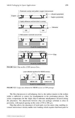
1. Fabricate overlay and pattern copper interconnects
Ultradel (polyimide)
Copper
Kapton (polyimide)
2. Apply adhesive and bond die to overlay
Adhesive
DIE DIE
3. Mold plastic substrate around die
DIE DIE
PLASTIC SUBSTRATE
4. Laser drill vias and sputtermetallization
Vias
DIE DIE
PLASTIC SUBSTRATE
FIGURE 12.4 Chip-on-flex (COF) process flow.
Laser ablated windows for MEMS access
MEMS DIE CMOS DIE
PLASTIC SUBSTRATE
FIGURE 12.5 Large area ablation for MEMS access in COF package.
The flip-chip process is self-aligning, that is, the surface tension in the molten
solder is sufficient to correct for misalignments in the positioning process. The
action compensates for the slight chip-to-substrate misalignment incurred during
die placement. The attachment between chip and package substrate is close in
proximity, with typical spacing on the order of 50 to 200 mm.
Flip-chip allows the placement of bond pads over the entire chip, enabling in-
creased interconnect density unlike wire bonding which requires that bond pads be
© 2006 by Taylor & Francis Group, LLC