
Page 283 - MEMS and Microstructures in Aerospace Applications
P. 283
Osiander / MEMS and microstructures in Aerospace applications DK3181_c012 Final Proof page 275 1.9.2005 9:13pm
MEMS Packaging for Space Applications 275
12.3 PACKAGE-TO-MEMS ATTACHMENT
The method used to attach a MEMS device to a package is a general technology
applicable to most integrated circuit (IC) devices. Generally referred to as die
attach, the function serves several critical functions. The main function is to provide
good mechanical attachment of the MEMS structure to the package base. This
ensures that the MEMS chip (or die) does not move relative to the package base. It
must survive hot and cold temperatures, moisture, shock, and vibration. The
attachment may also be required to provide a good thermal path between the
MEMS structure and the package base. Should heat be generated by the MEMS
structure or by the support circuitry, the attachment material should be able to
conduct the heat from the chip to the package base. The heat can be conducted away
from the chip and ‘‘spread’’ to the package base, which is larger and has more
thermal mass. This spread can keep the device operating in the desired temperature
range. If the support circuitry requires good electrical contact from the silicon to the
package base, the attachment material should be able to accommodate the task.
The stability and reliability of the attach material are largely dictated by the ability
of the material to withstand thermomechanical stresses created by the differences in
the CTE between the MEMS silicon and the package base material. These stresses are
concentrated at the interface between the MEMS silicon backside and the attach
material and the interface between the die-attach material and the package base as
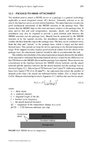
shown in Figure 12.1. Silicon has a CTE between 2 and 3 ppm/8C while most package
bases have higher CTE (6 to 20 ppm/8C). An expression that relates the number of
thermal cycles that a die attach can withstand before failure, N(f), is based on the
Coffin–Manson relationship for strain. Equation (12.1) defines the case for die attach:
m
2t
m
N( f) / g (12:1)
LDCTEDT
where
g ¼ shear strain
m ¼ material constant
L ¼ diagonal length of the die
f ¼ thermal cycle frequency
t ¼ die-attach material thickness
DT ¼ magnitude of the temperature change in a cycle
DCTE ¼ CTE between substrate and chip
Compressive
stress MEMS device
Die attach material
Package base
FIGURE 12.1 MEMS device in compression.
© 2006 by Taylor & Francis Group, LLC