
Page 362 - MEMS and Microstructures in Aerospace Applications
P. 362
Osiander / MEMS and microstructures in Aerospace applications DK3181_c016 Final Proof page 355 1.9.2005 12:56pm
Microelectromechanical Systems and Microstructures in Aerospace 355
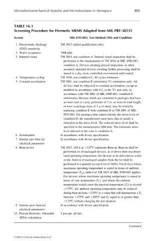
TABLE 16.1
Screening Procedure for Hermetic MEMS Adapted from MIL-PRF-38535
Screen MIL-STD-883, Test Method (TM) and Condition
1. Electrostatic discharge TM 3015 (initial qualification only)
(ESD) sensitivity
2. Wafer acceptance TRB plan
3. Internal visual TM 2010, test condition A. Internal visual inspection shall be
performed to the requirements of TM 2010 of MIL-STD-883,
condition A. Devices awaiting preseal inspection, or other
accepted, unsealed devices awaiting further processing shall be
stored in a dry, inert, controlled environment until sealed.
4. Temperature cycling TM 1010, test condition C, 50 cycles minimum
5. Constant acceleration TM 2001, test condition E (minimum) Y1 orientation only. All
devices shall be subjected to constant acceleration, except as
modified in accordance with 4.2, in the Y1 axis only, in
accordance with TM 2001 of MIL-STD-883, condition E
(minimum). Devices which are contained in packages that have
an inner seal or cavity perimeter of 2 in. or more in total length,
or have a package mass of 5 g or more, may be tested by
replacing condition E with condition D in TM 2001 of MIL-
STD-883. For packages that cannot tolerate the stress level of
condition D, the manufacturer must have data to justify a
reduction in the stress level. The reduced stress level shall be
specified in the manufacturers QM plan. The minimum stress
level allowed in this case is condition A.
6. Serialization In accordance with device specification
7. Interim (pre burn-in) In accordance with device specification
electrical parameters
8. Burn-in test TM 1015, 160 h at þ1258C minimum Burn-in. Burn-in shall be
performed on all packaged devices, at or above their maximum
rated operating temperature (for devices to be delivered as wafer
or die, burn-in of packaged samples from the lot shall be
performed to a quantity accept level of 10(0)). For devices whose
maximum operating temperature is stated in terms of ambient
temperature (T A ), table I of TM 1015 of MIL-STD-883 applies.
For devices whose maximum operating temperature is stated in
terms of case temperature (T C ), and where the ambient
temperature would cause the junction temperature (T J ) to exceed
þ1758C, the ambient operating temperature may be reduced
during burn-in from þ1258C to a value that will demonstrate a T J
between þ1758C and þ2008C and T C equal to or greater than
þ1258C without changing the test duration.
9. Interim (post burn-in) In accordance with device specification
electrical parameters
10. Percent Defective Allowable 5 percent, all lots
(PDA) calculation
Continued
© 2006 by Taylor & Francis Group, LLC