
Page 363 - MEMS and Microstructures in Aerospace Applications
P. 363
Osiander / MEMS and microstructures in Aerospace applications DK3181_c016 Final Proof page 356 1.9.2005 12:56pm
356 MEMS and Microstructures in Aerospace Applications
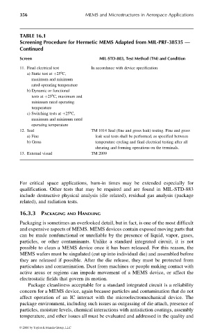
TABLE 16.1
Screening Procedure for Hermetic MEMS Adapted from MIL-PRF-38535 —
Continued
Screen MIL-STD-883, Test Method (TM) and Condition
11. Final electrical test In accordance with device specification
a) Static test at þ258C,
maximum and minimum
rated operating temperature
b) Dynamic or functional
tests at þ258C, maximum and
minimum rated operating
temperature
c) Switching tests at þ258C,
maximum and minimum rated
operating temperature
12. Seal TM 1014 Seal (fine and gross leak) testing. Fine and gross
a) Fine leak seal tests shall be performed, as specified between
b) Gross temperature cycling and final electrical testing after all
shearing and forming operations on the terminals.
13. External visual TM 2009
For critical space applications, burn-in times may be extended especially for
qualification. Other tests that may be required and are found in MIL-STD-883
include destructive physical analysis (die related), residual gas analysis (package
related), and radiation tests.
16.3.3 PACKAGING AND HANDLING
Packaging is sometimes an overlooked detail, but in fact, is one of the most difficult
and expensive aspects of MEMS. MEMS devices contain exposed moving parts that
can be made nonfunctional or unreliable by the presence of liquid, vapor, gases,
particles, or other contaminants. Unlike a standard integrated circuit, it is not
possible to clean a MEMS device once it has been released. For this reason, the
MEMS wafers must be singulated (cut up into individual die) and assembled before
they are released if possible. After the die release, they must be protected from
particulates and contamination. Dust from machines or people making contact with
active areas or regions can impede movement of a MEMS device, or affect the
electrostatic fields that govern its motion.
Package cleanliness acceptable for a standard integrated circuit is a reliability
concern for a MEMS device, again because particles and contamination that do not
affect operation of an IC interact with the microelectromechanical device. The
package environment, including such issues as outgassing of die attach, presence of
particles, moisture levels, chemical interactions with antistiction coatings, assembly
temperature, and other issues all must be evaluated and addressed in the quality and
© 2006 by Taylor & Francis Group, LLC