
Page 364 - MEMS and Microstructures in Aerospace Applications
P. 364
Osiander / MEMS and microstructures in Aerospace applications DK3181_c016 Final Proof page 357 1.9.2005 12:56pm
Microelectromechanical Systems and Microstructures in Aerospace 357
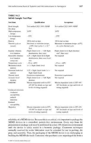
TABLE 16.2
MEMS Sample Test Plan
Test Item Qualification Acceptance
Bond strength Test method 2023 100% NDBP Test method 2023 100% NDBP
Die shear
High-temperature 1508C 1508C
storage
Low-temperature 558C 558C
storage
Burn-in 100 h total on-time 100 h total on-time
Thermal cycle or Maximum or minimum design Maximum or minimum design +158C;
5
vacuum +108C; four cycles 1 10 six cycles thermal cycle
Torr
Random vibration Flight (limit) level þ 3 dB flight Flight (limit) level flight duration/
1
level duration duration/axis; three axes axis ; three axes
Sinusoidal vibration 1.25 flight (limit) level flight Not required
level duration duration/axis; three axes 4 oct/
sweep rate min
Temperature cycle 55 to þ808C 55 to þ 608C
Mechanical shock 1.4 flight (limit) level Not required
analysis
Structural loads test 1.25 flight (limit) loads 1.4 Not required
analysis flight (limit) loads
Thermal shock Permission requirements Permission requirements
Acoustics level Flight (limit) level þ 3 dB flight Not required
duration duration
EMI/EMC Mission dependent (refer to ST5- Mission dependent (refer to ST5-495-
495-007 for details on type and 007 for details on type and levels of
levels of testing required) testing required)
Conducted emissions
conducted
susceptibility
radiated
emissions
Radiated
susceptibility
Magnetics Mission dependent (refer to ST5- Mission dependent (refer to ST5-495-
495-007 for details on type and 007 for details on type and levels of
levels of testing required) testing required)
reliability of a MEMS device. Because this is so critical, it is important to package the
MEMS devices in a controlled, particle-free environment. Every step from die
preparation to package seal must be performed in a class 100 cleanroom environment
until the device is safely sealed in a hermetic package. Cleanroom techniques
normally reserved for wafer fabrication must be extended for use in probing, die
prep, and assembly. Thus, the packaging of the MEMS device is as challenging as
building the MEMS die itself. Customers who purchase a raw unpackaged die from a
© 2006 by Taylor & Francis Group, LLC