
Page 59 -
P. 59
3-14 MEMS: Design and Fabrication
[001]
a
a
{100}
{111} Flat
a
{110} {110}
[100]
<110>
{111} {110}
[010]
{100} <110>
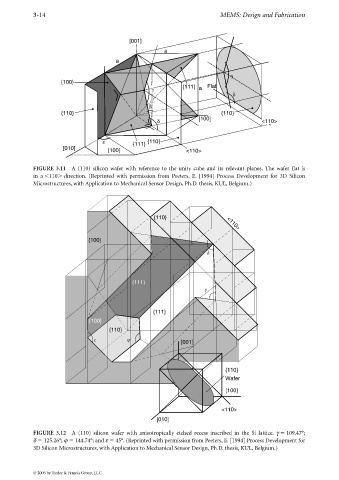
FIGURE 3.11 A (110) silicon wafer with reference to the unity cube and its relevant planes. The wafer flat is
in a 110 direction. (Reprinted with permission from Peeters, E. [1994] Process Development for 3D Silicon
Microstructures, with Application to Mechanical Sensor Design, Ph.D. thesis, KUL, Belgium.)
{110} <110>
{100}
{111}
{111}
{100}
{110}
[001]
{110}
Wafer
[100]
<110>
[010]
FIGURE 3.12 A (110) silicon wafer with anisotropically etched recess inscribed in the Si lattice. γ 109.47°;
δ 125.26°; ϕ 144.74°; and ε 45°. (Reprinted with permission from Peeters, E. [1994] Process Development for
3D Silicon Microstructures, with Application to Mechanical Sensor Design, Ph.D. thesis, KUL, Belgium.)
© 2006 by Taylor & Francis Group, LLC