
Page 54 -
P. 54
MEMS Fabrication 3-9
<110 >
{111}
[001] a
a
<110> <110>
{111}
Flat {110}
a
L
{100}
[100]
<110> [010]
<110>
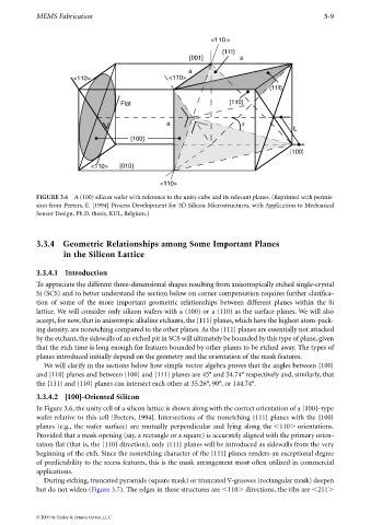
FIGURE 3.6 A (100) silicon wafer with reference to the unity cube and its relevant planes. (Reprinted with permis-
sion from Peeters, E. [1994] Process Development for 3D Silicon Microstructures, with Application to Mechanical
Sensor Design, Ph.D. thesis, KUL, Belgium.)
3.3.4 Geometric Relationships among Some Important Planes
in the Silicon Lattice
3.3.4.1 Introduction
To appreciate the different three-dimensional shapes resulting from anisotropically etched single-crystal
Si (SCS) and to better understand the section below on corner compensation requires further clarifica-
tion of some of the more important geometric relationships between different planes within the Si
lattice. Wewillconsider only silicon wafers with a (100) or a (110) as the surface planes. We will also
accept, for now, that in anisotropic alkaline etchants, the {111} planes, which have the highest atom-pack-
ing density, are nonetching compared to the other planes. As the {111} planes are essentially not attacked
by the etchant, the sidewalls of an etched pit in SCS will ultimately be bounded by this type of plane, given
that the etch time is long enough for features bounded by other planes to be etched away. The types of
planes introduced initially depend on the geometry and the orientation of the mask features.
We will clarify in the sections below how simple vector algebra proves that the angles between {100}
and {110} planes and between {100} and {111} planes are 45° and 54.74° respectively and, similarly, that
the {111} and {110} planes can intersect each other at 35.26°, 90°, or 144.74°.
3.3.4.2 [100]–Oriented Silicon
In Figure 3.6, the unity cell of a silicon lattice is shown along with the correct orientation of a [100]–type
wafer relative to this cell [Peeters, 1994]. Intersections of the nonetching {111} planes with the {100}
planes (e.g., the wafer surface) are mutually perpendicular and lying along the 110 orientations.
Provided that a mask opening (say, a rectangle or a square) is accurately aligned with the primary orien-
tation flat (that is, the [110] direction), only {111} planes will be introduced as sidewalls from the very
beginning of the etch. Since the nonetching character of the {111} planes renders an exceptional degree
of predictability to the recess features, this is the mask arrangement most often utilized in commercial
applications.
During etching, truncated pyramids (square mask) or truncated V-grooves (rectangular mask) deepen
but do not widen (Figure 3.7). The edges in these structures are 110 directions, the ribs are 211
© 2006 by Taylor & Francis Group, LLC