
Page 50 -
P. 50
MEMS Fabrication 3-5
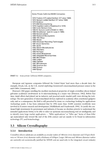
Some Private California MEMS Companies
1972 Foxboro ICT (called SenSym ICT since 1999)
1972 Sensym (called SenSym ICT since 1999)
1975 Endevco
1975 IBM Micromachining
1976 Cognition (sold to Rosemount in 1978)
1980 Irvine Sensors Corp.
1982 IC Sensors (sold to EG&G in 1994)
1985 NovaSensor (sold to Lucas in 1990)
1988 Nanostructures
1988 Redwood Microsystems
1988 TiNi Alloys
1989 Abaxis
1989 Advanced Recording Technologies
1991 Incyte Genomics
1991 Sentir
1992 Silicon Microstructures
1993 Affymetrix
1993 Nanogen
1995 Aclara Biosciences
1995 Integrated Micromachines
1995 MicroScape
1996 Caliper
1996 Cepheid
1997 Microsensors
1998 Quantum Dot
1998 Zyomyx
1999 Symyx
INSET 3.2 Some private California MEMS companies.
European and Japanese companies followed the United States’ lead more than a decade later; for
example, Druck, Ltd., in the U.K. started exploiting Greenwood’s micromachined pressure sensor in the
mid-1980s [Greenwood, 1984].
Petersen’s 1982 paper extolling the excellent mechanical properties of single-crystalline silicon helped
galvanize academia’s involvement in Si micromachining in a major way [Peterson, 1982]. Before that
time, timid efforts had played out in industry, and practical needs (market pull) were driving the tech-
nology. The new generation of micromachined devices explored in academia often constituted gadgetry
only, and as a consequence, the field is still perceived by many as a technology looking for applications
(technology push). It has been estimated that by 1994 more than 10,000 scientists worldwide were
involved in Si sensor research and development [Middlehoek and Dauderstadt, 1994]. To justify the con-
tinued high investments by government and industry, it became an absolute priority to understand the
intended applications better, to be able to select an optimum micromachining tool set intelligently, and
to identify more large market applications — “killer applications,” or “killer aps.” Some of these killer
aps materialized only toward the end of the 20th century and are mainly to be found in information
technology (IT) and biotechnology.
3.3 Silicon Crystallography
3.3.1 Introduction
Crystalline silicon substrates are available as circular wafers of 100mm (4 in) diameter and 525µm thick-
ness or 150 mm (6in) diameter with a thickness of 650µm. Larger 200 mm and 300mm diameter wafers
are currently not economically justified for MEMS and are used only in the integrated circuit industry
© 2006 by Taylor & Francis Group, LLC