
Page 47 -
P. 47
3-2 MEMS: Design and Fabrication
3.16 Surface Micromachining Processes ............................3-130
Basic Process Sequence • Fabrication Step Details • Control
of Film Stress • Dimensional Uncertainties • Sealing
Processes in Surface Micromachining • IC Compatibility
3.17 Poly-Si Surface Micromachining Modifications ......3-145
Porous Poly-Si • Hinged Polysilicon • Thick Polysilicon
• Milli-Scale Molded Polysilicon Structures
3.18 Surface Micromachining Modifications Not Involving
Polysilicon ....................................................................3-152
SOI Surface Micromachining • Resists as Structural
Elements and Molds in Surface Micromachining
3.19 Comparison of Bulk Micromachining with Surface
Micromachining ..........................................................3-161
3.20 Materials Case Studies ................................................3-163
Introduction • Polysilicon Deposition and Material Structure
• Amorphous and Hydrogenated Amorphous Silicon • Silicon
Nitride • CVD Silicon Dioxides • Metals in Surface
Guangyao Jia and Micromachining • Polycrystalline Diamond and SiC Films
Marc J. Madou 3.21 Polysilicon Surface Micromachining Examples ........3-181
University of California, Irvine
3.1 Wet Bulk Micromachining: Introduction
In wet bulk micromachining, features are sculpted in the bulk of materials such as silicon, quartz, SiC,
GaAs, InP, and Ge by orientation-independent (isotropic) or orientation-dependent (anisotropic) wet
etchants. The technology employs pools of liquid as tools [Harris, 1976] rather than dry etching plasmas.
A vast majority of wet bulk micromachining work is based on single-crystal silicon and glass as a com-
panion material. There has been some work on quartz, crystalline Ge, SiC, and GaAs, and a minor
amount on GaP and InP.
Wet bulk micromachining, along with surface micromachining, form the principal commercial Si
micromachining tool sets used today. Micromolding — from a lithography-defined master — has only
Deposit photoresist Open contacts
Silicon wafer
UV light
Deposit aluminum
Mask
Develop resist Pattern aluminum
Implant
boron Pattern back oxide
Anneal and oxidation Silicon etch
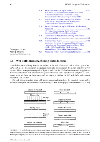
FIGURE 3.1 A wet bulk micromachining process is used to craft a membrane with piezoresistive elements. Silicon
micromachining selectively thins the double-sided polished silicon wafer from a starting thickness of about 425µm. A
diaphragm having a typical thickness of 20µm or less with precise lateral dimensions and vertical thickness control results.
© 2006 by Taylor & Francis Group, LLC