
Page 52 -
P. 52
MEMS Fabrication 3-7
[001]
a <100>
a
a
{100}
{100}
[100]
[010]
{100}
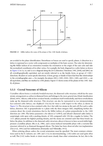
FIGURE 3.3 Miller indices for some of the planes of the {100} family of planes.
are avoided in the plane identification. Parentheses or braces are used to specify planes. A direction in a
lattice is expressed as a vector with components as multiples of the basis vectors. The rules for determin-
ing the Miller indices of an orientation translate the orientation to the origin of the unit cube and take
the normalized coordinates of its other vertex. For example, the body diagonal in a cubic lattice as shown
in Figure 3.2 is 1a,1a, and 1a or a diagonal along the [111] direction. Directions [100], [010], and [001] are
all crystallographically equivalent and are jointly referred to as the family, form, or group of 100
directions. Brackets or carets specify directions. A form, group, or family of faces that bear like relationships
to the crystallographic axes — for example, the planes (001), (100), (010), (001), (100), and (010) — are
all equivalent, and they are marked as {100} planes. Figure 3.3 shows some of the planes of the {100} fam-
ily of planes.
3.3.3 Crystal Structure of Silicon
Crystalline silicon forms a covalently bonded structure, the diamond-cubic structure, which has the same
atomic arrangement as carbon in diamond form and belongs to the more general zinc-blend classification
[Kittel, 1976]. Silicon, with its four covalent bonds, coordinates itself tetrahedrally, and these tetrahedrons
make up the diamond-cubic structure. This structure can also be represented as two interpenetrating
face-centered cubic lattices, one displaced (1/4,1/4,1/4) times a with respect to the other, as shown in
Figure 3.4. The structure is face-centered cubic (fcc), but with two atoms in the unit cell. For such a cubic
lattice, direction [hkl] is perpendicular to a plane with the three integers (hkl), simplifying further dis-
cussions about the crystal orientation; that is, the Miller indices of a plane perpendicular to the [100]
direction are (100). The lattice parameter a for silicon is 5.4309Å, and silicon’s diamond-cubic lattice is
surprisingly wide open with a packing density of 34% compared with 74% for a regular fcc lattice. The
{111} planes present the highest packing density, and the atoms are oriented such that three bonds are
below the plane. In addition to the diamond-cubic structure, silicon is known to have several stable high-
pressure crystalline phases [Hu et al., 1986], and a stress-induced metastable phase with a wurtzite-like
structure referred to as diamond-hexagonal silicon. The latter has been observed after ion implantation
[Tan et al., 1981] and hot indentation [Eremenko and Nikitenko, 1972].
When ordering silicon wafers, the crystal orientation must be specified. The most common orienta-
tions used in the IC industry are [100] and [111]; in micromachining, [110] wafers are used quite often
as well. The [110] wafers break or cleavemuch more cleanly than other orientations. In fact, this is the
© 2006 by Taylor & Francis Group, LLC