Page 56 -
P. 56

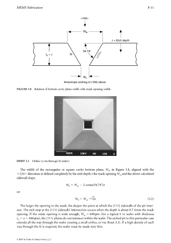
MEMS Fabrication                                                                           3-11


                                                         <100>


                                                           W m


                                                                               z = Etch depth


                                                           54.74°
                                 t  = z           Si                 <111>
                                 si


                                                           W
                                                             o
                                             Anisotropic etching of (100) silicon

             FIGURE 3.8 Relation of bottom cavity plane width with mask opening width.


             INSET 3.3 Orifice (a via through Si wafer).


               The  width  of the  rectangular  or  square  cavity  bottom  plane, W , in  Figure  3.8, aligned  with  the
                                                                             0
              110  directions is defined completely by the etch depth z the mask opening W and the above-calculated
                                                                                    m
             sidewall slope:

                                               W   W   2 cotan(54.74°)z
                                                       m
                                                 0
             or:

                                                     W   W   2 z                                        (3.2)
                                                       0     m
               The larger the opening in the mask, the deeper the point at which the {111} sidewalls of the pit inter-
             sect. The etch stop at the {111} sidewalls’ intersection occurs when the depth is about 0.7 times the mask
             opening. If the oxide opening is wide enough, W   849µm (for a typical 6 in wafer with thickness
                                                           m
             t   z   600µm), the {111} planes do not intersect within the wafer. The etched pit in this particular case
             si
             extends all the way through the wafer creating a small orifice, or via (Inset 3.3). If a high density of such
             vias through the Si is required, the wafer must be made very thin.


             © 2006 by Taylor & Francis Group, LLC
   51   52   53   54   55   56   57   58   59   60   61