
Page 57 -
P. 57
3-12 MEMS: Design and Fabrication
<110>
{111}
[001] a
<110> <110>
{111}
Flat
a {100}
{100}
[100]
<110> [010]
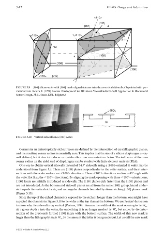
FIGURE 3.9 [100] silicon wafer with [100] mask-aligned features introduces vertical sidewalls. (Reprinted with per-
mission from Peeters, E. [1994] Process Development for 3D Silicon Microstructures, with Application to Mechanical
Sensor Design, Ph.D. thesis, KUL, Belgium.)
FIGURE 3.10 Vertical sidewalls in a (100) wafer.
Corners in an anisotropically etched recess are defined by the intersection of crystallographic planes,
and the resulting corner radius is essentially zero. This implies that the size of a silicon diaphragm is very
well defined, but it also introduces a considerable stress concentration factor. The influence of the zero
corner radius on the yield load of diaphragms can be studied with finite element analysis (FEA).
One way to obtain vertical sidewalls instead of 54.7° sidewalls using a [100]–oriented Si wafer may be
understood from Figure 3.9. There are {100} planes perpendicular to the wafer surface, and their inter-
sections with the wafer surface are 100 directions. These 100 directions enclose a 45° angle with
the wafer flat (i.e., the 110 directions). By aligning the mask opening with these 100 orientations,
{100} facets are initially introduced as sidewalls. The {110} planes etch faster than the {100} planes and
are not introduced. As the bottom and sidewall planes are all from the same {100} group, lateral under-
etch equals the vertical etch rate, and rectangular channels bounded by slower etching {100} planes result
(Figure 3.10).
Since the top of the etched channels is exposed to the etchant longer than the bottom, one might have
expected the channels in Figure 3.10 to be wider at the top than at the bottom. We use Peeters’ derivation
to show why the sidewalls stay vertical [Peeters, 1994]. Assume the width of the mask opening to be W .
m
At a given depth z into the wafer, the underlying Si is no longer masked by W but rather by the inter-
m
section of the previously formed {100} facets with the bottom surface. The width of this new mask is
larger than the lithography mask W by the amount the latter is being undercut. Let us call the new mask
m
© 2006 by Taylor & Francis Group, LLC