
Page 53 -
P. 53
3-8 MEMS: Design and Fabrication
FIGURE 3.4 The diamond-type lattice can be constructed from two interpenetrating face-centered cubic unit cells.
Si forms four covalent bonds making tetrahedrons.
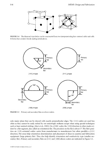
Primary Primary
flat flat
45°
Secondary
flat
[111] n-type [111] p-type
180°
Primary Primary
flat flat
90°
Secondary
flat Secondary
flat
[100] n-type [100] p-type
FIGURE 3.5 Primary and secondary flats on silicon wafers.
only major plane that can be cleaved with exactly perpendicular edges. The [111] wafers are used less
often as they cannot be easily etched by wet anisotropic etchants except when using special techniques
such as laser-assisted etching [Alavi et al., 1992]. On a [100] wafer, the [110] direction is often made evi-
dent by a flat segment, also called an orientation flat. The precision on the flat is about 3°. The flat’s posi-
tion on [110]–oriented wafers varies from manufacturer to manufacturer but often parallels a [111]
direction. Flat areas help orientation determination and placement of slices in cassettes and fabrication
equipment (large primary flat). They also help identify orientation and conductivity type (smaller sec-
ondary flat). Primary and secondary flats on [111] and [100] silicon wafers are indicated in Figure 3.5.
© 2006 by Taylor & Francis Group, LLC