
Page 55 -
P. 55
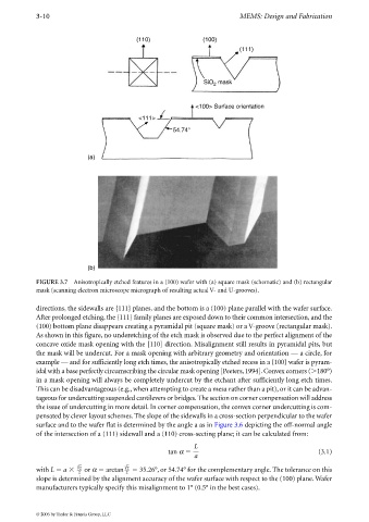
3-10                                                             MEMS: Design and Fabrication


                                             (110)                (100)
                                                                              (111)


                                                                   SiO  mask
                                                                      2


                                                                <100> Surface orientation
                                              <111>

                                                         54.74°


                             (a)


                             (b)
             FIGURE 3.7 Anisotropically etched features in a (100) wafer with (a) square mask (schematic) and (b) rectangular
             mask (scanning electron microscope micrograph of resulting actual V- and U-grooves).


             directions, the sidewalls are {111} planes, and the bottom is a (100) plane parallel with the wafer surface.
             After prolonged etching, the {111} family planes are exposed down to their common intersection, and the
             (100) bottom plane disappears creating a pyramidal pit (square mask) or a V-groove (rectangular mask).
             As shown in this figure, no underetching of the etch mask is observed due to the perfect alignment of the
             concave oxide mask opening with the [110] direction. Misalignment still results in pyramidal pits, but
             the mask will be undercut. For a mask opening with arbitrary geometry and orientation — a circle, for
             example — and for sufficiently long etch times, the anisotropically etched recess in a {100} wafer is pyram-
             idal with a base perfectly circumscribing the circular mask opening [Peeters, 1994]. Convex corners ( 180°)
             in a mask opening will always be completely undercut by the etchant after sufficiently long etch times.
             This can be disadvantageous (e.g., when attempting to create a mesa rather than a pit), or it can be advan-
             tageous for undercutting suspended cantilevers or bridges. The section on corner compensation will address
             the issue of undercutting in more detail. In corner compensation, the convex corner undercutting is com-
             pensated by clever layout schemes. The slope of the sidewalls in a cross-section perpendicular to the wafer
             surface and to the wafer flat is determined by the angle a as in Figure 3.6 depicting the off-normal angle
             of the intersection of a (111) sidewall and a (110) cross-secting plane; it can be calculated from:
                                                                L
                                                       tan α                                            (3.1)
                                                                a

                           2              2
             with L   a      or α   arctan      35.26°, or 54.74° for the complementary angle. The tolerance on this
                          2               2
             slope is determined by the alignment accuracy of the wafer surface with respect to the (100) plane. Wafer
             manufacturers typically specify this misalignment to 1° (0.5° in the best cases).


             © 2006 by Taylor & Francis Group, LLC