
Page 262 - Mechanical Engineers' Handbook (Volume 2)
P. 262
12 Programmable Interconnects 251
11 PROGRAMMABLE I/O BLOCKS
An I/O interface block is peripheral logic built to interface the chip to external devices
through its package pins. The term programmable indicates that the pins can be programmed
for a wide variety of I/O standards such as an input, output, or bidirectional. In state-of-the-
art FPGA devices, these I/O resources are typically grouped into banks. The compatibility
of these standards is based on the standard’s supply and reference voltage requirements. In
complicated designs that use more than one standard, complications arise that lead to con-
strained I/O pad placement issues, such as not being able to place certain I/O pads in the
same bank. This is a real problem if there is only one bank in the design. Current FPGAs
support several I/O standards. For example, some standards require use of a differential
amplifier input. With this standard, the external reference voltage must be applied to the
amplifier. This is an advantage in that it reduces the I/O voltages swings, which allows for
faster switching. Another standard may require a power supply for the I/O blocks. Figure
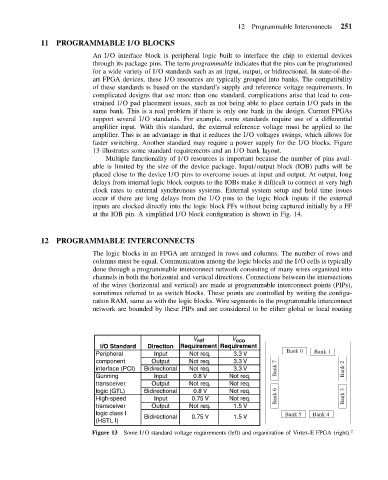
13 illustrates some standard requirements and an I/O bank layout.
Multiple functionality of I/O resources is important because the number of pins avail-
able is limited by the size of the device package. Input/output block (IOB) paths will be
placed close to the device I/O pins to overcome issues at input and output. At output, long
delays from internal logic block outputs to the IOBs make it difficult to connect at very high
clock rates to external synchronous systems. External system setup and hold time issues
occur if there are long delays from the I/O pins to the logic block inputs if the external
inputs are clocked directly into the logic block FFs without being captured initially by a FF
at the IOB pin. A simplified I/O block configuration is shown in Fig. 14.
12 PROGRAMMABLE INTERCONNECTS
The logic blocks in an FPGA are arranged in rows and columns. The number of rows and
columns must be equal. Communication among the logic blocks and the I/O cells is typically
done through a programmable interconnect network consisting of many wires organized into
channels in both the horizontal and vertical directions. Connections between the intersections
of the wires (horizontal and vertical) are made at programmable interconnect points (PIPs),
sometimes referred to as switch blocks. These points are controlled by writing the configu-
ration RAM, same as with the logic blocks. Wire segments in the programmable interconnect
network are bounded by these PIPs and are considered to be either global or local routing
V ref V cco
I/O Standard Direction Requirement Requirement
Bank 0 Bank 1
Peripheral Input Not req. 3.3 V
component Output Not req. 3.3 V
interface (PCI) Bidirectional Not req. 3.3 V Bank 7 Bank 2
Gunning Input 0.8 V Not req.
transceiver Output Not req. Not req.
logic (GTL) Bidirectional 0.8 V Not req.
High-speed Input 0.75 V Not req. Bank 6 Bank 3
transceiver Output Not req. 1.5 V
logic class I Bidirectional 0.75 V 1.5 V Bank 5 Bank 4
(HSTL I)
Figure 13 Some I/O standard voltage requirements (left) and organization of Virtex-E FPGA (right). 2