Page 391 - Mechanical Engineers' Handbook (Volume 4)
P. 391
380   Cooling Electronic Equipment

                          encountered in the flow of dissipated heat from the active chip surface through the materials
                          used to support and bond the chip and on to the case of the integrated circuit package. The
                          flow of heat from the case directly to the coolant, or indirectly through a fin structure and
                          then to the coolant, must overcome the external resistance, R .
                                                                          ex
                             The thermal design of single-chip packages, including the selection of die-bond, heat
                          spreader, substrate, and encapsulant materials, as well as the quality of the bonding and
                          encapsulating processes, can be characterized by the internal, or so-called junction–to–case,
                          resistance. The convective heat removal techniques applied to the external surfaces of the
                          package, including the effect of finned heat sinks and other thermal enhancements, can be
                          compared on the basis of the external thermal resistance. The complexity of heat flow and
                          coolant flow paths in a multichip module generally requires that the thermal capability of
                          these packaging configurations be examined on the basis of overall, or chip-to-coolant, ther-
                          mal resistance.

                          Internal Thermal Resistance
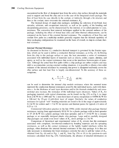
                          As discussed in Section 1.2, conductive thermal transport is governed by the Fourier equa-
                          tion, which can be used to define a conduction thermal resistance, as in Eq. (3). In flowing
                          from the chip to the package surface or case, the heat encounters a series of resistances
                          associated with individual layers of materials such as silicon, solder, copper, alumina, and
                          epoxy, as well as the contact resistances that occur at the interfaces between pairs of mate-
                          rials. Although the actual heat flow paths within a chip package are rather complex and may
                          shift to accommodate varying external cooling situations, it is possible to obtain a first-order
                          estimate of the internal resistance by assuming that power is dissipated uniformly across the
                          chip surface and that heat flow is largely one-dimensional. To the accuracy of these as-
                          sumptions,

                                                     T   T c     x
                                                      j
                                                R                     (K/W)                   (25)
                                                 jc
                                                       q c      kA
                          can be used to determine the internal chip module resistance where the summed terms
                          represent the conduction thermal resistances posed by the individual layers, each with thick-
                          ness x. As the thickness of each layer decreases and/or the thermal conductivity and cross-
                          sectional area increase, the resistance of the individual layers decreases. Values of R cd  for
                          packaging materials with typical dimensions can be found via Eq. (25) or Fig 4, to range
                                                2
                          from 2 K/W for a 1000-mm by 1-mm-thick layer of epoxy encapsulant to 0.0006 K/W for
                                  2
                          a 100-mm by 25- m (1-mil)-thick layer of copper. Similarly, the values of conduction
                          resistance for typical ‘‘soft’’ bonding materials are found to lie in the range of approximately
                          0.1 K/W for solders and 1–3 K/W for epoxies and thermal pastes for typical x/A ratios of
                          0.25 to 1.0.
                             Commercial fabrication practice in the late 1990s yields internal chip package thermal
                          resistances varying from approximately 80 K/W for a plastic package with no heat spreader
                          to 15–20 K/W for a plastic package with heat spreader, and to 5–10 K/W for a ceramic
                          package or an especially designed plastic chip package. Large and/or carefully designed
                          chip packages can attain even lower values of R , down perhaps to 2 K/W.
                                                                jc
                             Comparison of theoretical and experimental values of R reveals that the resistances
                                                                           jc
                          associated with compliant, low-thermal-conductivity bonding materials and the spreading
                          resistances, as well as the contact resistances at the lightly loaded interfaces within the
                          package, often dominate the internal thermal resistance of the chip package. It is thus not
                          only necessary to determine the bond resistance correctly but also to add the values of R ,
                                                                                                sp
                          obtained from Eq. (6) and/or Fig. 1, and R from Eq. (7b) or (9) to the junction–to–case
                                                            co
                          resistance calculated from Eq. (25). Unfortunately, the absence of detailed information on

