
Page 80 -
P. 80
2.5 Designs for Related Problems of an ESEC LD 69
2.0
Deflection (nm) 1.0
0.2
0.1
0 1.0 2.0 3.0
Thickness of a semiconductor film (mm)
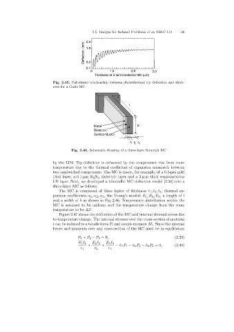
Fig. 2.45. Calculated relationship between photothermal tip deflection and thick-
ness for a GaAs MC
l
Metal b
Dielectric
Semiconductor
t t t 3
1 2
Fig. 2.46. Schematic drawing of a three-layer bimorph MC
by the LD2. Tip deflection is enhanced by the temperature rise from room
temperature due to the thermal coefficient of expansion mismatch between
two sandwiched components. The MC is made, for example, of a 0.1-µm gold
(Au) layer, a 0.1-µmSi 3 N 4 dielectric layer and a 2-µ m thick semiconductor
LD layer. Next, we developed a bimetallic MC deflection model [2.30] into a
three-layer MC as follows.
The MC is composed of three layers of thickness t 1 ,t 2 ,t 3 , thermal ex-
pansion coefficients α 1 ,α 2 ,α 3 , the Young’s moduli E 1 ,E 2 ,E 3 , a length of l
and a width of b as shown in Fig. 2.46. Temperature distribution within the
MC is assumed to be uniform and the temperature change from the room
temperature to be ∆T.
Figure 2.47 shows the deflection of the MC and internal thermal stress due
to temperature change. The internal stresses over the cross-section of material
i can be reduced to a tensile force P i and couple moment M i . Since the internal
forces and moments over any cross-section of the MC must be in equilibrium
P 1 + P 2 − P 3 =0, (2.29)
E 1 I 1 E 2 I 2 E 3 I 3
+ + − h 1 P 1 − h 2 P 2 − h 3 P 3 =0, (2.30)
r 1 r 2 r 3