Page 84 -
P. 84

2.5 Designs for Related Problems of an ESEC LD  73
                            Therefore, the total r and t are given as

                                                          r 012 + z 1 r 23 e −i2β 2
                                                      r =                 ,               (2.38)
                                                           1 − r 210 r 23 e −i2β 2
                                                            t 012 t 23 e −i2β 2
                                                       t =               .                (2.39)
                                                          1 − r 210 r 23 e −i2β 2
                                                where z 1 = t 012 t 210 − r 012 r 210 .   (2.40)
                            Consequently, the total energy reflectivity R and total energy transmission T
                            are given as
                                                            ∗
                                                      R = rr ,                            (2.41)
                                                          N 3 cos θ 3  ∗
                                                      T =         tt .                    (2.42)
                                                          N 2 cos θ 2
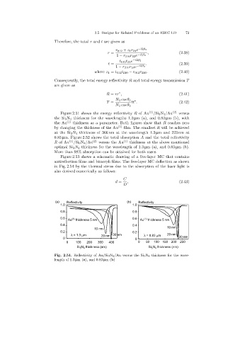
                               Figure 2.51 shows the energy reflectivity R of Au (1) /Si 3 N 4 /Au (2)  versus
                            the Si 3 N 4 thickness for the wavelengths 1.3 µm (a), and 0.83 µm (b), with
                            the Au (1)  thickness as a parameter. Both figures show that R reaches zero
                            by changing the thickness of the Au (1)  film. The smallest R will be achieved
                            at the Si 3 N 4 thickness of 366 nm at the wavelength 1.3 µm and 223 nm at
                            0.83 µm. Figure 2.52 shows the total absorption A and the total reflectivity
                            R of Au (1) /Si 3 N 4 /Au (2)  versus the Au (1)  thickness at the above mentioned
                            optimal Si 3 N 4 thickness for the wavelength of 1.3 µm (a), and 0.83 µm (b).
                            More than 98% absorption can be attained for both cases.
                               Figure 2.53 shows a schematic drawing of a five-layer MC that contains
                            antireflection films and bimorph films. The five-layer MC deflection as shown
                            in Fig. 2.54 by the thermal stress due to the absorption of the laser light is
                            also derived numerically as follows:

                                                              C
                                                          d =   ,                         (2.43)
                                                              D


                            (a)   Reflectivity                  (b)   Reflectivity
                               1.0                                 1.0
                               0.8                                 0.8
                               0.6  Au  thickness 5 nm             0.6  Au  thickness 5 nm
                                                                        (1)
                                     (1)
                               0.4                                 0.4
                                                10 nm                               10 nm
                               0.2                                 0.2
                                    l = 1.3 mm     20 nm  30 nm         l = 0.83 mm  20 nm
                                0                                   0                     30 nm
                                  0    100  200   300  400           0   50  100  150  200  250
                                       Si N  thickness (nm)                Si N  thickness (nm)
                                                                            3 4
                                         3 4
                            Fig. 2.51. Reflectivity of Au/Si 3N 4/Au versus the Si 3N 4 thickness for the wave-
                            length of 1.3 µm(a),and 0.83 µm(b)
   79   80   81   82   83   84   85   86   87   88   89