
Page 87 -
P. 87
76 2 Extremely Short-External-Cavity Laser Diode
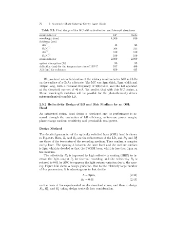
Table 2.2. Final design of the MC with antirefrection and bimorph structures
semiconductor InP GaAs
wavelength (nm)1,300 830
thickness (nm)
Au (1) 16 26
Si 3N (1) 366 223
4
Au (2) 100 100
Si 3N (2) 100 100
4
semiconductor 2,000 2,000
optical absorption (%)98 99
deflection (nm)for the temperature rise of 100 C 767 486
◦
λ/2 (nm)for reference 650 415
We produced a trial fabrication of the solitary semiconductor MC and LDs
on the surface of a GaAs substrate. The MC was 3 µmthick,5 µm width and
110 µm long, with a resonant frequency of 200.6 kHz, and the LD operated
at the threshold current of 46 mA. We predict that with this MC design, a
30-nm wavelength variation will be possible for the photothermally driven
micromechanical tunable LD.
2.5.2 Reflectivity Design of LD and Disk Medium for an OSL
Head
An integrated optical head design is developed and its performance is as-
sessed through the evaluation of LD efficiency, write-erase power margin,
phase change medium sensitivity and permissible read power.
Design Method
The detailed parameter of the optically switched laser (OSL) head is shown
l
in Fig. 2.35. Here, R 1 and R 2 are the reflectivities of the LD, and R and R h 3
3
are those of the two states of the recordingmedium. They confirm a complex
cavity laser. The spacing h between the laser facet and the medium surface
is 2 µm which is decided as that the FWHM beam width is less than 1 µmon
the medium.
The reflectivity R 1 is improved by high reflectivity coating (HRC) to in-
crease the light output P 2 for thermal recording, and the reflectivity R 2 is
reduced to 0.01 by ARC to suppress the light output variation due to the spac-
ing. Figure 2.56 shows a design guideline. Due to the relatively large number
of free parameters, it is advantageous to first decide
h =2 µm, (2.44)
R 2 =0.01 (2.45)
on the basis of the experimental results described above, and then to design
h
l
R 1 , R ,and R takingdesign tradeoffs into consideration.
3
3