Page 85 -
P. 85

74    2 Extremely Short-External-Cavity Laser Diode
                            (a)  Absorption A, Reflectivity R  (b)   Absorption A, Reflectivity R
                               1.0                                1.0

                               0.8               Si N  366 nm     0.8             Si N  223 nm
                                                  3 4
                                                                                    3 4
                               0.6                                0.6          R
                                              R
                               0.4                                0.4
                                                  A                              A
                               0.2                                0.2               l = 0.83 mm
                                                   l = 1.3 mm
                                          26 nm                           16 nm
                                0                                  0
                                 0    20   40   60   80   100        0   20   40   60   80  100
                                                                            (1)
                                         (1)
                                       Au  thickness (nm)                 Au  thickness (nm)
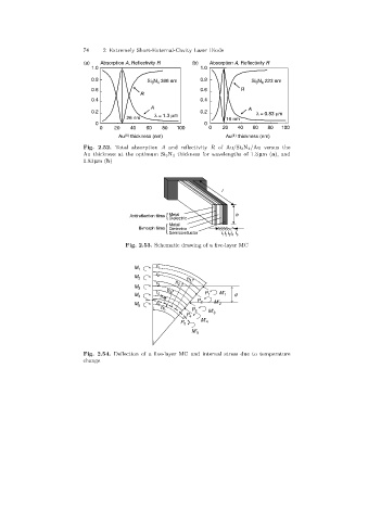
                            Fig. 2.52. Total absorption A and reflectivity R of Au/Si 3N 4/Au versus the
                            Au thickness at the optimum Si 3N 4 thickness for wavelengths of 1.3 µm(a),and
                            0.83 µm(b)


                                                                         l


                                           Antireflection films { Metal      b
                                                        Dielectric
                                                       { Metal
                                              Bimorph films Dielectric
                                                        Semiconductor    t t t t t
                                                                         1 2 3 4 5
                                          Fig. 2.53. Schematic drawing of a five-layer MC


                                            M 1    r 1
                                                   r
                                            M 2     2        h
                                                   r      h 2  1
                                            M 3     3
                                                   r   h 3         P    M’
                                            M 4     4 h 4           1     1  d
                                            M 5     r 5          P 2  M’ 2
                                                     h 5       P 3  M’
                                                             P 4      3
                                                           P 5    M’ 4
                                                               M’ 5


                            Fig. 2.54. Deflection of a five-layer MC and internal stress due to temperature
                            change
   80   81   82   83   84   85   86   87   88   89   90