
Page 82 -
P. 82
2.5 Designs for Related Problems of an ESEC LD 71
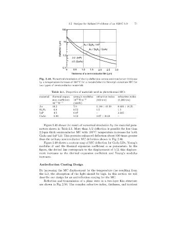
100
Deflection (mm) 10 Au / Si N / InP
3 4
Au / Si N / GaAs
3 4
1.0
l/2 (InP)
l/2 (GaAs)
0.1
0 0.5 1.0 1.5 2.0 2.5 3.0
Thickness of a semiconductor film (mm)
Fig. 2.48. Numerical simulation of the tip deflection versus semiconductor thickness
by a temperature increase of 100 C for a metal-dielectric bimorph structure MC for
◦
two types of semiconductor materials
Table 2.1. Properties of materials used in photothermal MCs
material thermal expan- young’s modulus refractive index refractive index
sion coefficient 10 10 Nm −2 (830 nm)(1,300 nm)
10 −6 K −1 (300 K)
Au 14.2 7.9 0.188 + i5.39 0.403 + i8.25
Si 3N 4 0.8 0.52 1.5 1.5
InP 4.5 6.07 – 3.205
GaAs 6.86 8.53 3.67 + i0.08 –
Figure 2.48 shows the result of numerical simulation by the material para-
meters shown in Table 2.1. More than λ/2 deflection is possible for less than
2.2-µm thick semiconductor MC with 100 C temperature increases for both
◦
GaAs and InP LD. This provides enhanced deflection about 500 times greater
than the solitary semiconductor MC deflection shown in Fig. 2.46.
Figure 2.49 shows a contour map of MC deflection for GaAs LDs, Young’s
modulus E and the thermal expansion coefficient α as parameters. In the
figure, the dotted line corresponds to the displacement of λ/2; this displace-
ment increases as the thermal expansion coefficient and Young’s modulus
increases.
Antireflection Coating Design
By increasingthe MC displacement by the temperature rise resultingfrom
the LD, the absorption of the light should be high. In this section we will
describe our design for an antireflection coating for the MC.
Reflection and transmission of a plane wave in a two-layer film structure
are shown in Fig. 2.50. The complex refractive index, thickness, and incident