
Page 230 - A Practical Guide from Design Planning to Manufacturing
P. 230
202 Chapter Seven
In the 1970s, processors were made using either just NMOS or just
PMOS devices, but starting in the 1980s chips were built using both. A
manufacturing process that creates N-type and P-type MOSFETs is
called complementary MOS (CMOS). Having NMOS and PMOS devices
allows logic gates to be designed where whenever one device turns on
another turns off. This way the output of the gate is always being pulled
to the supply voltage or ground but never both. These two voltages are
used to represent the 1’s and 0’s of binary numbers. Any instruction or
piece of data can be encoded as a number, and any number can be rep-
resented as a binary number using only two voltages.
The main reason why computers use binary is to keep circuit design
simple. It would be possible to design a processor that used more than
two voltage levels to represent each digit of a number. Ten voltage levels
per digit would allow numbers to be stored in decimal notation as we
are used to writing them. This would allow a smaller number of digits
to be used to represent each number, but the circuits processing those
digits would become enormously more complicated. Distinguishing
between 10 input voltage levels and producing the correct value of 10
possible output voltages would require treating the transistors as analog
devices. Many more transistors would be required to process each digit,
and these circuits would become much more susceptible to electrical noise.
Even though binary circuits require using more digits, they perform com-
putations faster at lower cost and vastly simplify the job of circuit design.
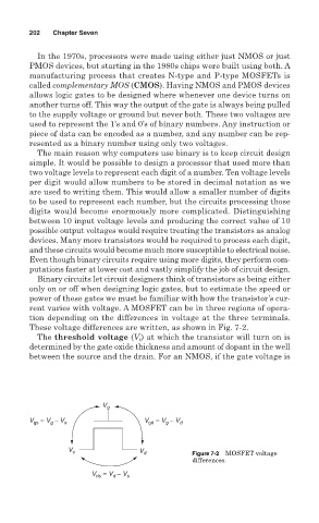
Binary circuits let circuit designers think of transistors as being either
only on or off when designing logic gates, but to estimate the speed or
power of these gates we must be familiar with how the transistor’s cur-
rent varies with voltage. A MOSFET can be in three regions of opera-
tion depending on the differences in voltage at the three terminals.
These voltage differences are written, as shown in Fig. 7-2.
) at which the transistor will turn on is
The threshold voltage (V t
determined by the gate oxide thickness and amount of dopant in the well
between the source and the drain. For an NMOS, if the gate voltage is
V g
V = V − V s V = V − V d
g
gd
gs
g
V s V d Figure 7-2 MOSFET voltage
differences.
V = V − V s
ds
d