
Page 235 - A Practical Guide from Design Planning to Manufacturing
P. 235
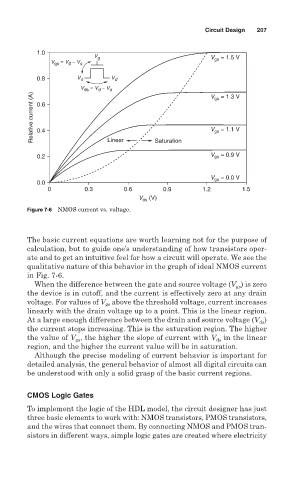
Circuit Design  207


           1.0
                          V g                             V gs  = 1.5 V
               V  = V g − V s
                gs
           0.8        V s      V d
                       V ds  = V d − V s                  V  = 1.3 V
          Relative current (A)  0.6                       V  = 1.1 V
                                                           gs


           0.4
                                                           gs

           0.2                Linear       Saturation     V  = 0.9 V
                                                           gs

                                                          V  = 0.0 V
                                                           gs
           0.0
              0         0.3        0.6       0.9        1.2       1.5
                                       V  (V)
                                        ds
        Figure 7-6 NMOS current vs. voltage.


        The basic current equations are worth learning not for the purpose of
        calculation, but to guide one’s understanding of how transistors oper-
        ate and to get an intuitive feel for how a circuit will operate. We see the
        qualitative nature of this behavior in the graph of ideal NMOS current
        in Fig. 7-6.
          When the difference between the gate and source voltage (V ) is zero
                                                                 gs
        the device is in cutoff, and the current is effectively zero at any drain
        voltage. For values of V above the threshold voltage, current increases
                              gs
        linearly with the drain voltage up to a point. This is the linear region.
        At a large enough difference between the drain and source voltage (V )
                                                                       ds
        the current stops increasing. This is the saturation region. The higher
        the value of V , the higher the slope of current with V ds  in the linear
                     gs
        region, and the higher the current value will be in saturation.
          Although the precise modeling of current behavior is important for
        detailed analysis, the general behavior of almost all digital circuits can
        be understood with only a solid grasp of the basic current regions.

        CMOS Logic Gates

        To implement the logic of the HDL model, the circuit designer has just
        three basic elements to work with: NMOS transistors, PMOS transistors,
        and the wires that connect them. By connecting NMOS and PMOS tran-
        sistors in different ways, simple logic gates are created where electricity