
Page 231 - A Practical Guide from Design Planning to Manufacturing
P. 231
Circuit Design 203
TABLE 7-1 MOSFET Current Equations
Region NMOS PMOS Current equation
Cutoff V gs < V t and V gd < V t V gs > V t and V gd > V t I ≈ 0
Saturation V gs > V t and V gd < V t V gs < V t and V gd > V t I ≈ 1 β( V − V t ) 2
gs
2
β
Linear V gs > V t and V gd > V t V gs < V t and V gd < V t I ≈ V − V t − V ds V ds
gs
2
not a threshold voltage above either the source or the drain, the transistor
will be off. This is called the cutoff region, and there will be almost no
current flow. If the gate voltage is a threshold voltage above the source but
not the drain, the transistor is said to be in saturation. In this case, the
channel formed beneath the gate will not reach all the way to the drain.
Current will flow but how much will be determined only by the voltages
at the source and gate. If the gate voltage is a threshold voltage above both
the source and drain, the transistor is in the linear region. The channel
will reach all the way from source to drain, and the current flowing will
be a function of the voltages on all three terminals. PMOS devices func-
tion in the same way but their threshold voltages are negative and the
gate voltage must be a threshold voltage below the source or drain to form
a channel (Table 7-1).
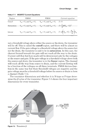
The transistor dimensions and whether it is N-type or P-type deter-
mine the b value of the transistor. Figure 7-3 shows the four important
dimensions for every transistor.
L gate
Poly m e Width
gate b = ox
Width T ox L eff
T ox
Source Drain
L eff
Well
Figure 7-3 Transistor b.