
Page 237 - A Practical Guide from Design Planning to Manufacturing
P. 237
Circuit Design 209
Inverter Inverter Inverter
circuit schematic schematic symbol truth table
In
In Out
In Out
0 1
Out 1 0
Figure 7-9 Inverter symbol and truth table.
through the PMOS to bring the output to a high voltage. When the volt-
age on the input is high (a logical 1), the PMOS transistor turns off and
the NMOS turns on. The NMOS drains away the charge on the output
returning it to a low voltage. Because the voltage on the output always
changes to the opposite of the voltage on the input, this circuit is called
an inverter. It inverts the binary signal on its input.
For commonly used logic gates, circuit designers use symbols as short-
hand for describing how the transistors are to be connected. The symbol
for an inverter is a triangle with a circle at the tip. The truth table for
a logic gate shows what the output will be for every possible combina-
tion of inputs. See Fig. 7-9. Because an inverter has only one input, its
truth table need only show two possible cases. More complicated logic
gates and behaviors can be created with more transistors.
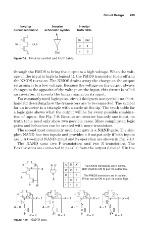
The second most commonly used logic gate is a NAND gate. The sim-
plest NAND has two inputs and provides a 0 output only if both inputs
are 1. A two-input NAND circuit and its operation are shown in Fig. 7-10.
The NAND uses two P-transistors and two N-transistors. The
P-transistors are connected in parallel from the output (labeled X in the
A B A B X The NMOS transistors are in series.
X 0 0 1 Both must be ON to pull the output low.
0 1 1 The PMOS transistors are in parallel.
A
X 1 0 1 Either can be ON to pull the output high.
B 1 1 0
X = 1 X = 1 X = 1 X = 0
A = 0 A = 0 A = 1 A = 1
B = 0 B = 1 B = 0 B = 1
Figure 7-10 NAND gate.