
Page 241 - A Practical Guide from Design Planning to Manufacturing
P. 241
Circuit Design 213
the supply voltage before a significant amount of noise is propagated to
its output.
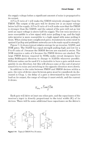
A P-to-N ratio of 1 will make the NMOS relatively stronger than the
PMOS. The output of the gate will be drawn low at an input voltage
below half the supply. A P-to-N ratio of 4 will make sure that the PMOS
is stronger than the NMOS, and the output of the gate will not go low
until an input voltage is above half the supply. The low ratio inverter is
more susceptible to a low signal with noise pulling it up, and the high
ratio inverter is more susceptible to a high signal with noise pulling it
down. When sizing more complicated gates, transistors in series must be
upsized if pullup and pulldown networks are to be made equal in strength.
Figure 7-14 shows typical relative sizings for an inverter, NAND, and
NOR gates. The NAND has equal strength pulling high and low for a
P-to-N ratio of 1 because the NMOS devices are stacked in series. The
NOR requires a ratio of 4 because the PMOS devices are stacked. The
large PMOS devices required by NORs make circuit designers favor
using DeMorgan’s theorem to change to NANDs wherever possible.
Different ratios can be used if it is desirable to have a gate switch more
quickly in one direction, but this will always come at the cost of greater
sensitivity to noise and switching in the opposite direction more slowly.
In addition to the ratio between PMOS and NMOS devices within a
gate, the ratio of device sizes between gates must be considered. As dis-
cussed in Chap. 1, the delay of a gate is determined by the capacitive
load on its output, the range of voltage it must switch, and the current
it draws.
T = C load × V dd
delay
I
Each gate will drive at least one other gate, and the capacitance of the
receiver’s input is directly proportional to the total width (W ) of its
r
devices. There will be some additional base capacitance on the driver’s
4
2 2
2
2 4
1
2 1 1
Figure 7-14 Typical CMOS P-to-N ratios.