Page 242 - A Practical Guide from Design Planning to Manufacturing
P. 242
214 Chapter Seven
output due to the total width of the drain diffusion (W d ) of the driver’s
own devices.
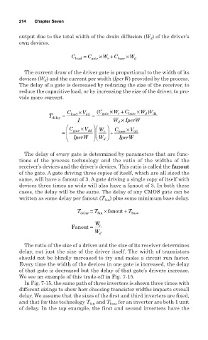
C = C × W + C × W
load gate r base d
The current draw of the driver gate is proportional to the width of its
devices (W ) and the current per width (IperW) provided by the process.
d
The delay of a gate is decreased by reducing the size of the receiver, to
reduce the capacitive load, or by increasing the size of the driver, to pro-
vide more current.
d
r
T = C load × V dd = ( C gate × W + C base × W V ) dd
delay
I W × IperW
I
d
C × V
= gate dd W r + C base ×V dd
IperW W IperW
d
The delay of every gate is determined by parameters that are func-
tions of the process technology and the ratio of the widths of the
receiver’s devices and the driver’s devices. This ratio is called the fanout
of the gate. A gate driving three copies of itself, which are all sized the
same, will have a fanout of 3. A gate driving a single copy of itself with
devices three times as wide will also have a fanout of 3. In both these
cases, the delay will be the same. The delay of any CMOS gate can be
written as some delay per fanout (T ) plus some minimum base delay.
fan
T delay = T fan × fanout + T base
Fanout = W r
W d
The ratio of the size of a driver and the size of its receiver determines
delay, not just the size of the driver itself. The width of transistors
should not be blindly increased to try and make a circuit run faster.
Every time the width of the devices in one gate is increased, the delay
of that gate is decreased but the delay of that gate’s drivers increase.
We see an example of this trade-off in Fig. 7-15.
In Fig. 7-15, the same path of three inverters is shown three times with
different sizings to show how choosing transistor widths impacts overall
delay. We assume that the sizes of the first and third inverters are fixed,
and that for this technology T fan and T base for an inverter are both 1 unit
of delay. In the top example, the first and second inverters have the

