
Page 243 - A Practical Guide from Design Planning to Manufacturing
P. 243
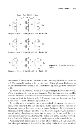
Circuit Design  215


                 T delay  = T fan  × fanout  + T base
                    T fan  = 1 and T base  = 1

                2           2         32
                    A          B
          In                             Out
                1           1         16


        Delay (In → A) = 2  Delay (A → B) = 17 Total = 19


                2          32        32
                    A          B
          In                             Out
                1          16        16

        Delay (In → A) = 17 Delay (A → B) = 2  Total = 19


                  2          8         32
                    A          B
          In                              Out
                  1          4         16       Figure 7-15 Sizing for minimum
                                                delay.
        Delay (In → A) = 5  Delay (A → B) = 5  Total = 10


        same sizes. The fanout is 1 and therefore the delay of the first inverter
        is 2. The second inverter is driving devices 16 times larger. Its fanout is
        16, and therefore the delay is 17. The total delay through both inverters
        is 19.
          To speed up this circuit, a circuit designer might increase the width
        of the transistors in the second inverter. This is shown in the middle
        example. Here the second inverter has been made the same size as the third
        inverter, so that its delay is only 2. However, now the delay of the first
        inverter is 17, so the total delay is still 19.
          To get the minimum delay, we must gradually increase the inverter
        sizes, as is shown in the last example. In the last example, the size of
        the second inverter has been chosen to make the fanout for both stages 4.
        This makes both delays 5 and the total delay 10. In general, to minimize
        overall delay, the designer must try to keep the fanout and delay at
        each gate roughly equal. Anytime the delay at a gate’s input is very dif-
        ferent from the delay on its output, resizing can reduce total delay.
          Assuming that gates have zero delay at zero fanout, it can be shown
        that the optimal fanout for minimizing delay is the irrational number