
Page 244 - A Practical Guide from Design Planning to Manufacturing
P. 244
216 Chapter Seven
1
e (≈ 2.718). Unfortunately real gates have some delay even with no load
at all. This makes the optimum fanout a function of the process tech-
nology, which will determine the ratio of the delay per fanout (T ) and
fan
the delay at zero fanout (T base ). Typical values for the optimal fanout of
an inverter are between 3 and 4. Because different types of logic gates
will have different values of T fan and T base , their optimal fanout will be
different. In general, as the number of gate inputs increases, the opti-
mal fanout of the gate goes down. The more complex the gate, the greater
its delay, and the less it should be loaded when optimizing for delay. The
final sizing for minimum delay will be a function of all the different types
of logic gates in the path as well as the loading due to interconnects
between the gates. Although CAD tools can find the optimal sizing for
simple paths through iteration, there is no analytical solution. An easy
way to spot inexperienced designers is to look for engineers making one
gate exactly 2.718 times the size of another.
Even if there were a single value for optimal fanout, it would be very
poor circuit design to always size for this value. Sizing for optimal fanout
is trying to minimize delay. However, some paths in any circuit block will
have more logic gates than others and therefore more delay. Only the very
slowest paths will limit the operating frequency, and only these paths
should be sized to minimize delay. Other paths can use smaller transis-
tors to reduce the die area and power needed. Device sizing is one of a cir-
cuit designer’s most powerful tools, but there is not a single perfect sizing
or single perfect logic gate.
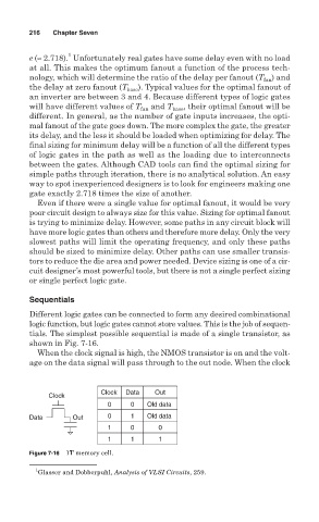
Sequentials
Different logic gates can be connected to form any desired combinational
logic function, but logic gates cannot store values. This is the job of sequen-
tials. The simplest possible sequential is made of a single transistor, as
shown in Fig. 7-16.
When the clock signal is high, the NMOS transistor is on and the volt-
age on the data signal will pass through to the out node. When the clock
Clock Data Out
Clock
0 0 Old data
Data Out 0 1 Old data
1 0 0
1 1 1
Figure 7-16 1T memory cell.
1
Glasser and Dobberpuhl, Analysis of VLSI Circuits, 259.