
Page 245 - A Practical Guide from Design Planning to Manufacturing
P. 245
Circuit Design 217
signal is low, the transistor will be off, and the capacitance of the out
node will hold the charge stored there. This is the memory cell used by
DRAM chips to form the main memory store of computers. This cell has
the advantage of using the minimum possible number of transistors and
therefore the minimum possible die area, but it has a number of disad-
vantages as well.
We have already noted that NMOS transistors cannot drive a node all
the way up to the supply voltage. This means that when writing a 1 into
the single transistor memory cell (1T memory cell), the voltage stored
on the out node will actually be one threshold voltage down from the volt-
age on the clock signal. Also, charge will tend to leak away from the out
node over time. With nothing to replace the charge, the data stored will
eventually be lost. DRAM chips deal with this problem by rewriting all
their data every 15 ms. Because of the signal loss when storing a high
voltage and the need for refreshing the cell, microprocessors do not use
the 1T memory cell for their sequentials. Instead, this circuit is altered
to form a more robust storage circuit, the latch. The changes needed to
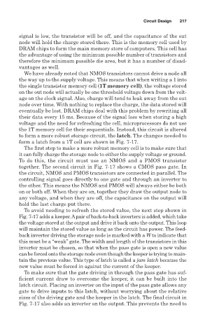
form a latch from a 1T cell are shown in Fig. 7-17.
The first step to make a more robust memory cell is to make sure that
it can fully charge the storage node to either the supply voltage or ground.
To do this, the circuit must use an NMOS and a PMOS transistor
together. The second circuit in Fig. 7-17 shows a CMOS pass gate. In
the circuit, NMOS and PMOS transistors are connected in parallel. The
controlling signal goes directly to one gate and through an inverter to
the other. This means the NMOS and PMOS will always either be both
on or both off. When they are on, together they draw the output node to
any voltage, and when they are off, the capacitance on the output will
hold the last charge put there.
To avoid needing to refresh the stored value, the next step shown in
Fig. 7-17 adds a keeper. Apair of back-to-back inverters is added, which take
the voltage stored at the output and drive it back onto the output. This loop
will maintain the stored value as long as the circuit has power. The feed-
back inverter driving the storage node is marked with a W to indicate that
this must be a “weak” gate. The width and length of the transistors in this
inverter must be chosen, so that when the pass gate is open a new value
can be forced onto the storage node even though the keeper is trying to main-
tain the previous value. This type of latch is called a jam latch because the
new value must be forced in against the current of the keeper.
To make sure that the gate driving in through the pass gate has suf-
ficient current draw to overcome the keeper, it can be built into the
latch circuit. Placing an inverter on the input of the pass gate allows any
gate to drive inputs to this latch, without worrying about the relative
sizes of the driving gate and the keeper in the latch. The final circuit in
Fig. 7-17 also adds an inverter on the output. This prevents the need to