
Page 249 - A Practical Guide from Design Planning to Manufacturing
P. 249
Circuit Design 221
for the desired application. All of these checks require modeling the true
electrical behavior of the transistors rather than simply treating them
as being on or off. To quickly and accurately model these behaviors for
large circuits, modern designers rely heavily upon CAD tools.
Timing
The area on which circuit designers typically spend the most effort is
circuit timing. Chapter 6 described how flip-flops act like stoplights
between the different stages of a processor pipeline. The same clock
signal is routed to all the flip-flops, and on its rising edge all the flip-
flops “turn green” and allow the signal at their input to pass through.
The signals rush through the logic of each pipestage toward the next flip-
flop. For proper operation, all the signals must have reached the next
flip-flop before the clock switches high again to mark the beginning of
the next cycle. The slowest possible path between flip-flops will deter-
mine the maximum processor frequency. It is therefore important to
balance the logic within each pipestage to make them all have roughly
the same delay. One fast pipestage is wasteful since the clock rate will
always be limited by whichever pipestage is slowest. The circuit design-
ers work toward the same clock frequency target, and circuits that are
too slow are said to have a maxdelay violation or a speedpath.
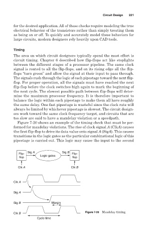
Figure 7-20 shows an example of the timing check that must be per-
formed for maxdelay violations. The rise of clock signal A (ClkA) causes
the first flip-flop to drive its data value onto signal A (SigA). This causes
transitions in the logic gates as the particular combinational logic of this
pipestage is carried out. This logic may cause the input to the second
Sig A Sig B
Flip- Flip-
Logic gates
flop flop
Clk A Clk B
Clk A
Sig A
Sig B Margin
Figure 7-20 Maxdelay timing.
Clk B
Cycle time