
Page 246 - A Practical Guide from Design Planning to Manufacturing
P. 246
218 Chapter Seven
Clock
1T DRAM cell Data Out
Clock
CMOS pass gate Data Out
W
Clock
Unbuffered latch Data Out
W
Clock
Buffered latch Data Out
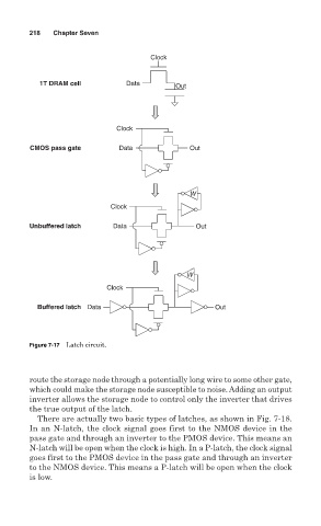
Figure 7-17 Latch circuit.
route the storage node through a potentially long wire to some other gate,
which could make the storage node susceptible to noise. Adding an output
inverter allows the storage node to control only the inverter that drives
the true output of the latch.
There are actually two basic types of latches, as shown in Fig. 7-18.
In an N-latch, the clock signal goes first to the NMOS device in the
pass gate and through an inverter to the PMOS device. This means an
N-latch will be open when the clock is high. In a P-latch, the clock signal
goes first to the PMOS device in the pass gate and through an inverter
to the NMOS device. This means a P-latch will be open when the clock
is low.