
Page 240 - A Practical Guide from Design Planning to Manufacturing
P. 240
212 Chapter Seven
parallel to make a gate switch when it is not supposed to. For performance
and noise immunity, it is better to implement logic requiring a large number
of inputs using multiple stages of small gates rather than a single very com-
plex CMOS gate.
Transistor sizing
Something on which circuit designers spend a great deal of time is choos-
ing the best size for each of the transistors in their circuits. Most tran-
sistors will be drawn at the minimum allowed length in order to provide
the most current when switching, but transistor widths must be chosen
to balance speed, area, power, and resistance to noise.
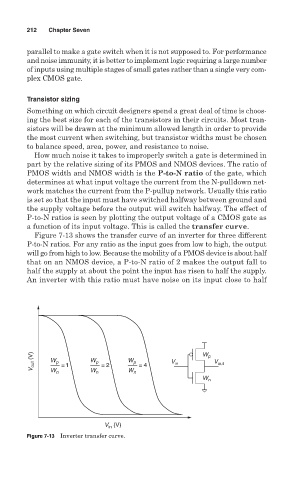
How much noise it takes to improperly switch a gate is determined in
part by the relative sizing of its PMOS and NMOS devices. The ratio of
PMOS width and NMOS width is the P-to-N ratio of the gate, which
determines at what input voltage the current from the N-pulldown net-
work matches the current from the P-pullup network. Usually this ratio
is set so that the input must have switched halfway between ground and
the supply voltage before the output will switch halfway. The effect of
P-to-N ratios is seen by plotting the output voltage of a CMOS gate as
a function of its input voltage. This is called the transfer curve.
Figure 7-13 shows the transfer curve of an inverter for three different
P-to-N ratios. For any ratio as the input goes from low to high, the output
will go from high to low. Because the mobility of a PMOS device is about half
that on an NMOS device, a P-to-N ratio of 2 makes the output fall to
half the supply at about the point the input has risen to half the supply.
An inverter with this ratio must have noise on its input close to half
V out (V) W p = 1 W p = 2 W p = 4 V in W p V out
W n
W n
W n
W n
V (V)
in
Figure 7-13 Inverter transfer curve.