
Page 337 - A Practical Guide from Design Planning to Manufacturing
P. 337
Microprocessor Packaging 307
Step #1 Step #2
Core layers Drill and pattern layers
FR4
Copper foil
Step #3 Step #4
Interleave prepeg layers Fuse layers
Apply heat
and pressure
Prepreg
Prepreg
Buried via
Blind via
Step #5 Step #6
Drill and pattern outer layers Mount and solder
Plated through Solder THT SMT
hole (PTH) mask package Solder package
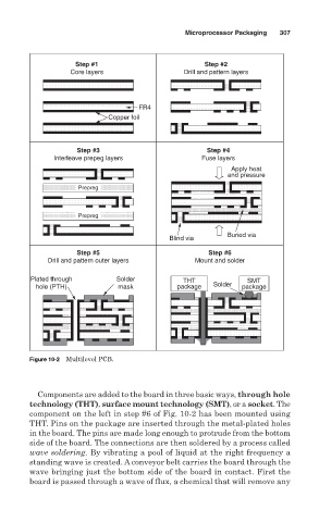
Figure 10-2 Multilevel PCB.
Components are added to the board in three basic ways, through hole
technology (THT), surface mount technology (SMT), or a socket. The
component on the left in step #6 of Fig. 10-2 has been mounted using
THT. Pins on the package are inserted through the metal-plated holes
in the board. The pins are made long enough to protrude from the bottom
side of the board. The connections are then soldered by a process called
wave soldering. By vibrating a pool of liquid at the right frequency a
standing wave is created. A conveyor belt carries the board through the
wave bringing just the bottom side of the board in contact. First the
board is passed through a wave of flux, a chemical that will remove any