
Page 336 - A Practical Guide from Design Planning to Manufacturing
P. 336
306 Chapter Ten
epoxy and makes a stiff substrate to form the basis of a PCB. Sheets that
have been already been impregnated with epoxy but not yet fully cured
are called prepreg. To allow at least two levels of wiring in the board,
the FR4 substrate usually has sheets of copper foil pressed on both
sides. Photoresist is deposited and developed on each side, and the
copper is etched to leave behind the desired traces. This is exactly the
same type of process used to pattern wiring levels on die, but to keep
costs down, PCBs rely on less advanced lithography and only wet etch-
ing. This means the tightest pitches on the board are typically much
larger than the wiring pitches on die.
Drilling holes in the board and plating them with metal creates vias.
Vias make connections between the wiring layers, and these same holes
are used to make connections to pinned packages. Circuit boards with a
large number of components or high-power components may require
more than two levels of traces. In a multilayer board, typically some of
the interconnect layers are dedicated to the high-voltage supply and
some to the low-voltage ground. These layers are often continuous sheets
of metal except where vias have been drilled through. Other layers are
dedicated to signal traces, which make input and output connections
between the components. Having sheets of metal at constant voltage
above or below the signal traces helps reduce electrical noise and allows
for higher bandwidth switching. The power and ground planes also help
provide a low-resistance path for delivering power to all the components.
Multiple two-sided boards can be combined to create multilevel boards.
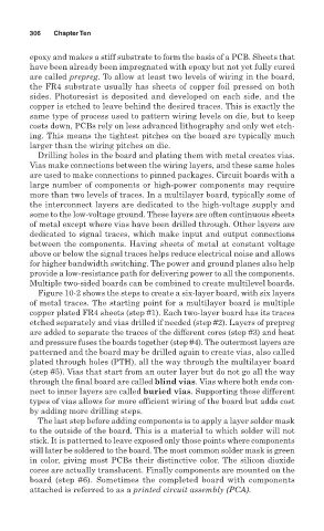
Figure 10-2 shows the steps to create a six-layer board, with six layers
of metal traces. The starting point for a multilayer board is multiple
copper plated FR4 sheets (step #1). Each two-layer board has its traces
etched separately and vias drilled if needed (step #2). Layers of prepreg
are added to separate the traces of the different cores (step #3) and heat
and pressure fuses the boards together (step #4). The outermost layers are
patterned and the board may be drilled again to create vias, also called
plated through holes (PTH), all the way through the multilayer board
(step #5). Vias that start from an outer layer but do not go all the way
through the final board are called blind vias. Vias where both ends con-
nect to inner layers are called buried vias. Supporting these different
types of vias allows for more efficient wiring of the board but adds cost
by adding more drilling steps.
The last step before adding components is to apply a layer solder mask
to the outside of the board. This is a material to which solder will not
stick. It is patterned to leave exposed only those points where components
will later be soldered to the board. The most common solder mask is green
in color, giving most PCBs their distinctive color. The silicon dioxide
cores are actually translucent. Finally components are mounted on the
board (step #6). Sometimes the completed board with components
attached is referred to as a printed circuit assembly (PCA).