
Page 376 - A Practical Guide from Design Planning to Manufacturing
P. 376
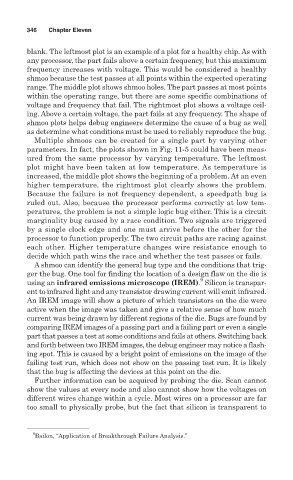
346   Chapter Eleven

        blank. The leftmost plot is an example of a plot for a healthy chip. As with
        any processor, the part fails above a certain frequency, but this maximum
        frequency increases with voltage. This would be considered a healthy
        shmoo because the test passes at all points within the expected operating
        range. The middle plot shows shmoo holes. The part passes at most points
        within the operating range, but there are some specific combinations of
        voltage and frequency that fail. The rightmost plot shows a voltage ceil-
        ing. Above a certain voltage, the part fails at any frequency. The shape of
        shmoo plots helps debug engineers determine the cause of a bug as well
        as determine what conditions must be used to reliably reproduce the bug.
          Multiple shmoos can be created for a single part by varying other
        parameters. In fact, the plots shown in Fig. 11-5 could have been meas-
        ured from the same processor by varying temperature. The leftmost
        plot might have been taken at low temperature. As temperature is
        increased, the middle plot shows the beginning of a problem. At an even
        higher temperature, the rightmost plot clearly shows the problem.
        Because the failure is not frequency dependent, a speedpath bug is
        ruled out. Also, because the processor performs correctly at low tem-
        peratures, the problem is not a simple logic bug either. This is a circuit
        marginality bug caused by a race condition. Two signals are triggered
        by a single clock edge and one must arrive before the other for the
        processor to function properly. The two circuit paths are racing against
        each other. Higher temperature changes wire resistance enough to
        decide which path wins the race and whether the test passes or fails.
          A shmoo can identify the general bug type and the conditions that trig-
        ger the bug. One tool for finding the location of a design flaw on the die is
                                                       9
        using an infrared emissions microscope (IREM). Silicon is transpar-
        ent to infrared light and any transistor drawing current will emit infrared.
        An IREM image will show a picture of which transistors on the die were
        active when the image was taken and give a relative sense of how much
        current was being drawn by different regions of the die. Bugs are found by
        comparing IREM images of a passing part and a failing part or even a single
        part that passes a test at some conditions and fails at others. Switching back
        and forth between two IREM images, the debug engineer may notice a flash-
        ing spot. This is caused by a bright point of emissions on the image of the
        failing test run, which does not show on the passing test run. It is likely
        that the bug is affecting the devices at this point on the die.
          Further information can be acquired by probing the die. Scan cannot
        show the values at every node and also cannot show how the voltages on
        different wires change within a cycle. Most wires on a processor are far
        too small to physically probe, but the fact that silicon is transparent to


          9
          Bailon, “Application of Breakthrough Failure Analysis.”