
Page 429 - Microsensors, MEMS and Smart Devices - Gardner Varadhan and Awadelkarim
P. 429
TESTING OF A MEMS-IDT ACCELEROMETER 409
Photoresist
Oxide 500 nm
p - type silicon wafer p-type silicon wafer
a. Oxidation b. Spin on photoresist
p-type silicon wafer p-type silicon wafer
d. Plasma etch Si to get
c. Pattern and develop photoresist
required spacer height
Spacer
100 nm,400 nm,
1 (im, 2 |o,m
p-type silicon wafer
e. Strip oxide to complete
spacer fabrication
f. Perspective view of device after
first stage of fabrication
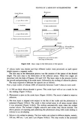
Figure 14.8 Basic steps in the fabrication of the spacers
4" silicon wafer was chosen and four different wafers were processed, as each spacer
height requires a separate wafer.
The first step in the fabrication process was the creation of the spacer of the desired
height. The next step is the fabrication of the reflector arrays. These two stages are
described with the help of Figures 14.8 and 14.9. The basic steps in the process involve
the growth and patterning of an oxide mask, followed by dry etching of silicon by plasma.
The steps required to fabricate the spacers are as follows:
Four p-type wafers of silicon (100) of resistivity between 2 and 5 ohm.cm were used.
1. A 500 nm thick silicon dioxide is grown. This oxide layer will act as a mask for the
dry etching (Figure 14.8(a)).
2. Photoresist is spun on the oxide layer (Figure 14.8(b)). The resist is baked to improve
adhesion.
3. The first mask is aligned with respect to the flat of the wafer and the photoresist is
patterned (Figure 14.8(c)). The oxide is then etched away in all areas except where
it was protected (Figure 14.8(d)). The etching automatically stops when the etchant
reaches silicon. The etchant is highly selective and etches only silicon dioxide. The
above process of exposing and patterning the photoresist along with oxide etching is
referred to as developing.
4. Silicon is dry-etched in plasma. The four wafers are etched to different depths, namely,
100 nm, 400 nm, 1 urn, and 2 um (Figure 14.8(e)). This step results in the protected