
Page 428 - Microsensors, MEMS and Smart Devices - Gardner Varadhan and Awadelkarim
P. 428
408 MEMS-IDT MICROSENSORS
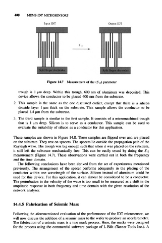
Figure 14.7 Measurement of the (Sj 2) parameter
trough is 1 \im deep. Within this trough, 600 nm of aluminum was deposited. This
device allows the conductor to be placed 400 nm from the substrate.
2. This sample is the same as the one discussed earlier, except that there is a silicon
dioxide layer 1 um thick on the substrate. This sample allows the conductor to be
placed 1.4 um from the substrate.
3. The third sample is similar to the first sample. It consists of a micromachined trough
that is 1 um deep. Silicon is to serve as a conductor. This sample can be used to
evaluate the suitability of silicon as a conductor for this application.
These samples are shown in Figure 14.8. These samples are flipped over and are placed
on the substrate. They rest on spacers. The spacers lie outside the propagation path of the
Rayleigh wave. The trough was big enough such that when it was placed on the substrate,
it still left the substrate mechanically free. This can be easily tested by doing the S\2
measurement (Figure 14.7). These observations were carried out in both the frequency
and the time domain.
The following conclusions have been derived from the set of experiments mentioned
previously. The arrangement of the spacer performs adequately in the placing of the
conductor within one wavelength of the surface. Silicon instead of aluminum could be
used for this device. For this application, it can almost be considered to be a conductor.
The perturbation in the velocity of the wave is too small to be measured as a shift in the
amplitude response in both frequency and time domain with the given resolution of the
network analyser.
14.4.5 Fabrication of Seismic Mass
Following the aforementioned evaluation of the performance of the IDT microsensor, we
will now discuss the addition of a seismic mass to the wafer to produce an accelerometer.
The fabrication of a seismic mass is a two mask process. Here, the masks were designed
for the process using the commercial software package of L-Edit (Tanner Tools Inc.). A