Page 426 - Microsensors, MEMS and Smart Devices - Gardner Varadhan and Awadelkarim
P. 426
406    MEMS-IDT  MICROSENSORS

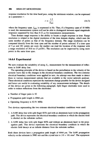
   response resolution  for the time band pass,  using the minimum window, can be  expressed
   as a parameter  r:
                                         1.2
                                    r = -—                              (14.3)
                                        f span

   where  the  frequency span  f span  is expressed  in  Hz. Thus,  if a  frequency  span of  10 MHz
   is used,  the measurement  system will not be able to distinguish  between  equal  magnitude
   responses  separated  by  less  than 0.12  us for  transmission  measurements.
     Time  domain  range  response  is the  ability  to  locate a  single  response in time.  Range
   resolution  is  related  to  the  digital  resolution  of  the  time domain  display,  which uses  the
   same  number  of  points  as  that  of  the  frequency  domain.  The  range  resolution  can  be
   computed  directly  from  the  time  span  and  the  number of  points  selected.  If a  time  span
   of  5  us  and  201  points  are  used,  the  marker  can  read  the  location  of  the  response  with
   a  range  resolution  of  24.8  ns  (5  us/201). The  resolution can  be  improved  by  using  more
   points  in  the  same  time span.


   14.4.4  Experimental

   We now evaluate the suitability of using  S 11  measurement for the  measurement of reflec-
   tions  in  SAW delay line.
     The operating  principle of the device  is based  on the perturbation in the velocity  of the
   acoustic  wave due to the changes  in the electrical  boundary conditions.  The two extreme
   electrical boundary conditions  were applied  in turn. An attempt was  then made  to  detect
  these  in  various  measurement  options  that  are  available  in  the  vector  network  analyser.
  These electrical  conditions represent the maximum change possible for the device  designed
   and  hence  are  useful  in evaluating suitability of  any  measurement technique.  The  details
  of  this  device  are  given in  the  following paragraph.  Split  finger  electrodes were  used  in
  order  to reduce  reflections from the electrodes:

   •  Number of finger pairs  is 10

  •  Propagation  path  length is 6944 urn
  •  Operating  frequency is 82.91 MHz

  Two devices  representing  the  two extreme electrical boundary conditions were  used:

   1.  A SAW delay line with split finger IDTs and with an aluminum layer in the  propagation
     path. This device represents  the electrical boundary condition in which the electric field
     is  shorted  on  the  substrate surface.
  2.  A  SAW delay  line with split  finger  IDTs and  without an aluminum layer  in the  prop-
     agation  path.  This  device  represents  the  electrical  boundary  condition  in  which  the
     electric  field  decays  at  an  infinite  distance  from  the  substrate surface.

  Both  these  devices  have  a  propagation  path  length  of  6944 urn. The  SAW  propagation
                                                               2
  velocity on the substrate is 3980  m/s and the crystal size is (10  x  10) mm . The equipment

