
Page 50 - Microsensors, MEMS and Smart Devices - Gardner Varadhan and Awadelkarim
P. 50
32 ELECTRONIC MATERIALS AND PROCESSING
Schematic of a medium-current
ion implanter
Resolving
Acceleration v- scan
High-voltage aperture
tube , p lates P lates Beam
terminal v. Wafer
mask
(target)
Analyzer
magnet
Faraday cup
Ion source
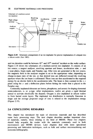
Figure 2.18 Schematic arrangement of an ion implanter for precise implantation of a dopant into
a silicon wafer (Sze 1985)
11
and ion densities could be between 10 and 10 16 ions/cm 2 incident on the wafer surface.
Figure 2.18 shows the schematics of a medium-current ion implanter. It consists of an
ion source, a magnet analyser, resolving aperture and lenses, acceleration tube, x- and
y-scan plates, beam mask, and Faraday cup. After ions are generated in the ion source,
the magnetic field in the analyser magnet is set to the appropriate value, depending on
charge-to-mass ratio of the ion, so that desired ions are deflected toward the resolving
aperture where the ion beam is collimated. These ions are then accelerated to the required
energy by an electric field in the acceleration tube. The beam is then scanned in the x-y
plane using the x- and y-deflection plates before hitting the wafer that is placed in the
Faraday cup.
Commonly implanted elements are boron, phosphorus, and arsenic for doping elemental
semiconductors, n- or p-type. After implantations, wafers are given a rapid thermal
anneal to activate electrically the dopants. Oxygen is also implanted in silicon wafers
to form buried oxide layers. The implanted ion distribution is normally Gaussian in
shape and the average projected range of ions is related to the implantation energy
(Figure 2.19).
2.6 CONCLUDING REMARKS
This chapter has introduced the topic of electronic materials and has described
some basic processing steps. The next chapter describes another important class
of materials, namely, those relating to the field of MEMS. These two chapters
should help acquaint the reader with the materials commonly used in both
microsensors and MEMS devices. Later chapters deal with more specialised
processing and fabrication techniques, such as bulk and surface micromachining and
stereomicrolithography.