
Page 47 - Microsensors, MEMS and Smart Devices - Gardner Varadhan and Awadelkarim
P. 47
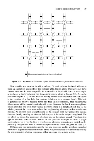
DOPING  SEMICONDUCTORS     29


                      Electron pair (bound electrons) in a covalent bond


      Figure  2.15  Hypothetical  2D  silicon  crystal  doped  with boron  (p-type  semiconductor)

     Now  consider  the  situation  in  which a  Group IV  semiconductor  is  doped  with atoms
  from  an  element  in  Group  III  of  the  periodic  table,  that  is,  atoms  that  have  only  three
  valence electrons.  To be more specific, let us take silicon doped with boron as an example,
  as  is  shown in  the  hypothetical  two-dimensional  silicon  lattice  in Figure  2.15.  As  can be
   seen  from  Figure  2.15,  the  net  effect  of  having a  boron  atom  that  substitutes  for  silicon
  is  the  creation  of  a  free  hole  (an  electron  deficiency  in  a  covalent  bond).  This  hole
  is  generated  as  follows:  because  boron  has  three  valence  electrons,  three neighbouring
   silicon atoms will be bonded covalently with boron. However, the fourth nearest-neighbour
  silicon  atom  has  one  of  its  four  valence electrons  sitting in  a  dangling bond;  that  is,  the
  whole system of the boron  atom and the four  neighbouring silicon  atoms has one electron
  missing.  An  electron  from  a neighbouring Si-Si  covalent  bond  may replace  the missing
  electron,  thereby  creating  an  electron  deficiency (a  hole)  at  the  neighbouring  bond.  The
  net  effect  is,  hence,  the  generation  of  a  free  hole  in  the  silicon  crystal.  Therefore,  this
  type  of  extrinsic  semiconductor,  silicon  in  this  particular  example,  is  called  a  p-type
  semiconductor  or  p-type  Si.  It  is  p-type  because  electrical  conduction  is  carried  out  by
  positively  charged  free  holes.  Common  acceptor  atoms  to  silicon  are given  in Table  2.7.
     Diffusion  and ion  implantation  are the  two key processes  used to introduce  controlled
  amounts of dopants into semiconductors.  These  two processes  are used to dope selectively
  the  semiconductor substrate to produce either an n-type or  a p-type region.