
Page 42 - Microsensors, MEMS and Smart Devices - Gardner Varadhan and Awadelkarim
P. 42
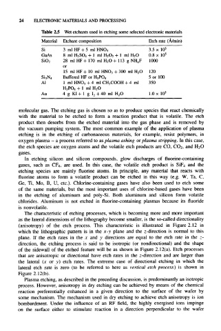
24    ELECTRONIC  MATERIALS AND PROCESSING

               Table 2.5 Wet etchants used  in etching  some  selected electronic  materials

               Material  Etchant  composition            Etch  rate (A/min)
               Si      3  ml HF +  5  ml HNO 3           3.5 x  10 5
               GaAs    8  ml H 2SO 4 +  1 ml H 2O 2 +  1 ml H 2O  0.8 x 10 5
                       28  ml HF +  170 ml H 2O +  113 g NH 4F  1000
               SiO 2
                       or
                       15  ml  HF -I- 10  ml  HNO 3 +  300  ml  H 2O  120
                       Buffered  HF or                   5 or  100
               Si 3N 4              H 3PO 4
               Al      1  ml HNO 3 + 4  ml CH 3COOH  + 4 ml  350
                             +  1  ml H 2O
                       H 3PO 4
               Au      4  g  KI +  1 g  I 2 + 40  ml H 2O  1.0 x  10 5


     molecular  gas.  The  etching  gas  is  chosen  so as  to  produce  species  that  react  chemically
     with  the  material  to  be  etched  to  form  a  reaction  product  that  is  volatile.  The  etch
     product  then  desorbs  from  the  etched  material  into  the  gas  phase  and  is  removed  by
     the  vacuum  pumping  system.  The  most  common  example  of  the  application  of  plasma
     etching  is  in  the  etching  of  carbonaceous  materials,  for  example,  resist  polymers,  in
     oxygen plasma  -  a process referred to as plasma ashing  or plasma stripping. In this case,
     the  etch  species are oxygen  atoms  and the  volatile  etch  products  are CO, CO 2,  and H2O
     gases.
        In  etching  silicon  and  silicon  compounds,  glow  discharges  of  fluorine-containing
     gases,  such  as  CF4,  are  used.  In  this  case,  the  volatile  etch  product  is  SiF 4  and  the
     etching  species  are  mainly  fluorine  atoms.  In  principle,  any  material  that  reacts  with
     fluorine  atoms  to  form  a  volatile  product  can  be  etched  in  this  way  (e.g.  W,  Ta,  C,
     Ge,  Ti,  Mo,  B,  U,  etc.).  Chlorine-containing  gases  have  also  been  used  to  etch  some
     of  the  same  materials,  but  the  most  important  uses  of  chlorine-based  gases  have  been
     in  the  etching  of  aluminum  and  poly-Si.  Both  aluminum  and  silicon  form  volatile
     chlorides.  Aluminum  is  not  etched  in  fluorine-containing  plasmas  because  its  fluoride
     is nonvolatile.
        The  characteristic  of  etching  processes,  which  is  becoming  more  and  more  important
     as the lateral dimensions  of the lithography  become smaller,  is the so-called  directionality
     (anisotropy)  of  the  etch  process.  This  characteristic  is  illustrated  in  Figure  2.12  in
     which  the  lithographic  pattern  is  in  the  x-y  plane  and  the  z-direction  is  normal  to  this
     plane.  If  the  etch  rates  in  the  x  and  y  directions  are  equal  to  the  etch  rate  in  the  z-
     direction,  the  etching  process  is  said  to  be  isotropic  (or  nondirectional)  and  the  shape
     of  the  sidewall  of  the  etched  feature  will  be  as  shown  in  Figure  2.12(a). Etch  processes
     that  are  anisotropic  or  directional  have  etch  rates  in  the  z-direction  and  are  larger  than
     the  lateral  (x  or  y)  etch  rates.  The  extreme  case  of  directional  etching  in  which  the
     lateral  etch  rate  is  zero  (to  be  referred  to  here  as  vertical  etch  process)  is  shown  in
     Figure  2. 12(b).
        Plasma etching, as described  in the preceding discussion, is predominantly an  isotropic
     process.  However,  anisotropy  in  dry  etching can  be  achieved  by  means  of  the  chemical
     reaction  preferentially  enhanced  in  a  given  direction  to  the  surface  of  the  wafer  by
     some  mechanism. The  mechanism  used  in  dry  etching to  achieve  etch  anisotropy  is  ion
     bombardment.  Under  the  influence  of  an  RF  field,  the  highly  energised  ions  impinge
     on  the  surface  either  to  stimulate  reaction  in  a  direction  perpendicular  to  the  wafer