
Page 45 - Microsensors, MEMS and Smart Devices - Gardner Varadhan and Awadelkarim
P. 45
DOPING SEMICONDUCTORS 27
5. Product desorption:
(adsorbed) (gas) (2.19)
SiCl n SiCl n
The final gas product is pumped out of the etching chamber. Table 2.6 provides a list of
etch gases used for dry-etching various electronic materials.
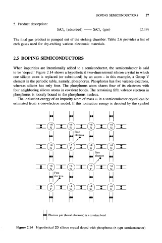
2.5 DOPING SEMICONDUCTORS
When impurities are intentionally added to a semiconductor, the semiconductor is said
to be 'doped.' Figure 2.14 shows a hypothetical two-dimensional silicon crystal in which
one silicon atom is replaced (or substituted) by an atom - in this example, a Group V
element in the periodic table, namely, phosphorus. Phosphorus has five valence electrons,
whereas silicon has only four. The phosphorus atom shares four of its electrons with
four neighboring silicon atoms in covalent bonds. The remaining fifth valence electron in
phosphorus is loosely bound to the phosphorus nucleus.
The ionisation energy of an impurity atom of mass m in a semiconductor crystal can be
estimated from a one-electron model. If this ionisation energy is denoted by the symbol
Electron pair (bound electrons) in a covalent bond
Figure 2.14 Hypothetical 2D silicon crystal doped with phosphorus (n-type semiconductor)