
Page 44 - Microsensors, MEMS and Smart Devices - Gardner Varadhan and Awadelkarim
P. 44
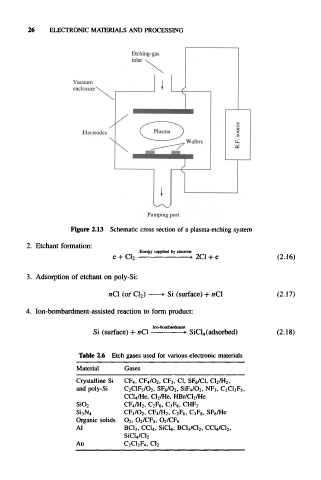
26    ELECTRONIC MATERIALS AND PROCESSING


                                  Etching-gas
                                  inlet


                  Vacuum
                  enclosure


                     Electrodes


                                       Pumping port

                 Figure  2.13  Schematic  cross section  of a plasma-etching  system

     2.  Etchant  formation:
                                    Energy  supplied by electron
                                                  >  2C1 + e                (2.16)
                             e + C1 2
     3.  Adsorption  of etchant  on poly-Si:

                            nCl  (or  C1 2 )  » Si  (surface) -I- nC\      (2.17)

     4.  lon-bombardment-assisted  reaction  to form  product:

                                        Ion-bombardment
                        Si (surface) +  nCl      > SiCl n(adsorbed)       (2.18)

                    Table 2.6  Etch gases  used  for various electronic materials

                   Material     Gases
                   Crystalline Si  CF 4,  CF 4/O 2,  CF 3,  Cl,  SF 6 /C1, C1 2/H 2,
                   and poly-Si  C 2C1F 5/O 2, SF 6/O 2,  SiF 4/O 2,  NF 3,  C 2Cl 3F 5,
                                CCl 4/He,  Cl 2/He,  HBr/Cl 2/He
                   Si0 2        CF 4/H 2, C 2F 6, C 3F 8,  CHF 3
                                CF 4/O 2,  CF 4/H 2, C 2F 6, C 3F 8, SF 6/He
                   Si 3N 4
                   Organic solids  O 2, O 2/CF 4,  O 2/CF 6
                   Al           BC1 3 , CCl 4, SiCl 4,  BC1 3 /C1 2 , CCl 4/Cl 2,
                                SiCl 4/Cl 2
                   Au           C 2C1 2F 4, C1 2