
Page 43 - Microsensors, MEMS and Smart Devices - Gardner Varadhan and Awadelkarim
P. 43
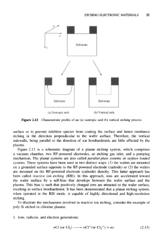
ETCHING ELECTRONIC  MATERIALS     25


                        (a) Isotropic etch       (b) Vertical etch

         Figure  2.12  Characteristic profile  of an  (a)  isotropic  and  (b)  vertical etching  process


     surface  or  to  prevent  inhibitor  species  from  coating  the  surface  and  hence  reenhance
     etching  in  the  direction  perpendicular  to  the  wafer  surface.  Therefore,  the  vertical
     sidewalls,  being  parallel  to  the  direction  of  ion  bombardment,  are  little  affected  by  the
     plasma.
       Figure  2.13  is  a  schematic  diagram  of  a  planar  etching  system,  which  comprises
     a  vacuum  chamber,  two  RF-powered  electrodes,  an  etching  gas  inlet,  and  a  pumping
     mechanism.  The  planar  systems  are  also  called  parallel-plate  systems  or  surface  loaded
     systems.  These  systems have been  used  in two  distinct  ways: (1) the  wafers are mounted
     on  a grounded  surface  opposite  to  the  RF-powered  electrode  (cathode)  or  (2)  the wafers
     are  mounted  on  the  RF-powered  electrode  (cathode)  directly.  This  latter  approach  has
     been  called  reactive  ion  etching  (RIE).  In  this  approach,  ions  are  accelerated  toward
     the  wafer  surface  by  a  self-bias  that  develops  between  the  wafer  surface  and  the
     plasma.  This  bias  is  such  that  positively  charged  ions  are  attracted  to  the  wafer  surface,
     resulting  in surface bombardment.  It has been  demonstrated  that a planar etching  system,
     when  operated  in  the  RIE  mode,  is  capable  of  highly  directional  and  high-resolution
     etching.
       To illustrate the  mechanisms involved in reactive ion etching, consider the example  of
     poly-Si  etched  in chlorine  plasma:

     1.  Ions, radicals,  and  electron generations:

                                              +
                                                     +
                              (or  C1 2)  > nCl (or C1 2 )  +  ne         (2.15)