
Page 40 - Microsensors, MEMS and Smart Devices - Gardner Varadhan and Awadelkarim
P. 40
22 ELECTRONIC MATERIALS AND PROCESSING
Radiation
Mask
Resist
Substrate
(b)
Deposit
Substrate Substrate
(c) (d)
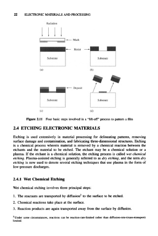
Figure 2.11 Four basic steps involved in a "lift-off' process to pattern a film
2.4 ETCHING ELECTRONIC MATERIALS
Etching is used extensively in material processing for delineating patterns, removing
surface damage and contamination, and fabricating three-dimensional structures. Etching
is a chemical process wherein material is removed by a chemical reaction between the
etchants and the material to be etched. The etchant may be a chemical solution or a
plasma. If the etchant is a chemical solution, the etching process is called wet chemical
etching. Plasma-assisted etching is generally referred to as dry etching, and the term dry
etching is now used to denote several etching techniques that use plasma in the form of
low-pressure discharges.
2.4.1 Wet Chemical Etching
Wet chemical etching involves three principal steps:
1. The reactants are transported by diffusion 2 to the surface to be etched.
2. Chemical reactions take place at the surface.
3. Reaction products are again transported away from the surface by diffusion.
2
Under some circumstances, reactions can be reaction-rate-limited rather than diffusion-rate-(mass-transport)
limited.