
Page 36 - Microsensors, MEMS and Smart Devices - Gardner Varadhan and Awadelkarim
P. 36
18 ELECTRONIC MATERIALS AND PROCESSING
45° mirror
/ x. \
Primary mirror
Mask . „ . „ ^ o
90° Roof mirror
Wafer
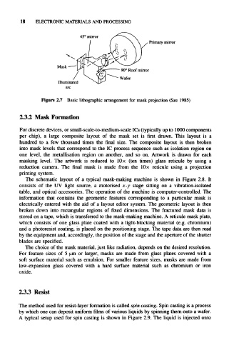
Figure 2.7 Basic lithographic arrangement for mask projection (Sze 1985)
2.3.2 Mask Formation
For discrete devices, or small-scale-to-medium-scale ICs (typically up to 1000 components
per chip), a large composite layout of the mask set is first drawn. This layout is a
hundred to a few thousand times the final size. The composite layout is then broken
into mask levels that correspond to the IC process sequence such as isolation region on
one level, the metallisation region on another, and so on. Artwork is drawn for each
masking level. The artwork is reduced to 10 x (ten times) glass reticule by using a
reduction camera. The final mask is made from the 10x reticule using a projection
printing system.
The schematic layout of a typical mask-making machine is shown in Figure 2.8. It
consists of the UV light source, a motorised x-y stage sitting on a vibration-isolated
table, and optical accessories. The operation of the machine is computer-controlled. The
information that contains the geometric features corresponding to a particular mask is
electrically entered with the aid of a layout editor system. The geometric layout is then
broken down into rectangular regions of fixed dimensions. The fractured mask data is
stored on a tape, which is transferred to the mask-making machine. A reticule mask plate,
which consists of one glass plate coated with a light-blocking material (e.g. chromium)
and a photoresist coating, is placed on the positioning stage. The tape data are then read
by the equipment and, accordingly, the position of the stage and the aperture of the shutter
blades are specified.
The choice of the mask material, just like radiation, depends on the desired resolution.
For feature sizes of 5 ^im or larger, masks are made from glass plates covered with a
soft surface material such as emulsion. For smaller feature sizes, masks are made from
low-expansion glass covered with a hard surface material such as chromium or iron
oxide.
2.3.3 Resist
The method used for resist-layer formation is called spin casting. Spin casting is a process
by which one can deposit uniform films of various liquids by spinning them onto a wafer.
A typical setup used for spin casting is shown in Figure 2.9. The liquid is injected onto