
Page 34 - Microsensors, MEMS and Smart Devices - Gardner Varadhan and Awadelkarim
P. 34
16 ELECTRONIC MATERIALS AND PROCESSING
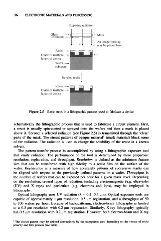
Figure 2.5 Basic steps in a lithographic process used to fabricate a device
schematically the lithographic process that is used to fabricate a circuit element. First,
a resist is usually spin-coated or sprayed onto the wafers and then a mask is placed
above it. Second, a selected radiation (see Figure 2.5) is transmitted through the 'clear'
parts of the mask. The circuit patterns of opaque material 1 (mask material) block some
of the radiation. The radiation is used to change the solubility of the resist in a known
solvent.
The pattern-transfer process is accomplished by using a lithographic exposure tool
that emits radiation. The performance of the tool is determined by three properties:
resolution, registration, and throughput. Resolution is defined as the minimum feature
size that can be transferred with high fidelity to a resist film on the surface of the
wafer. Registration is a measure of how accurately patterns of successive masks can
be aligned with respect to the previously defined patterns on a wafer. Throughput is
the number of wafers that can be exposed per hour for a given mask level. Depending
on the resolution, several types of radiation, including electromagnetic (e.g. ultraviolet
(UV) and X rays) and paniculate (e.g. electrons and ions), may be employed in
lithography.
Optical lithography uses UV radiation (A ~ 0.2-0.4 urn). Optical exposure tools are
capable of approximately 1 um resolution, 0.5 urn registration, and a throughput of 50
to 100 wafers per hour. Because of backscattering, electron-beam lithography is limited
to a 0.5 um resolution with 0.2 um registration. Similarly, X-ray lithography typically
has 0.5 um resolution with 0.2 um registration. However, both electron-beam and X-ray
1
The circuit pattern may be defined alternatively by the transparent part, depending on the choice of resist
polarity and film process (see later).