
Page 32 - Microsensors, MEMS and Smart Devices - Gardner Varadhan and Awadelkarim
P. 32
14 ELECTRONIC MATERIALS AND PROCESSING
dichlorosilane can be used as follows:
900°C
SiCl 2H 2 + 2H 2O SiO 2 + 2H 2 + 2HC1 (2.4)
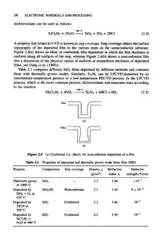
A property that relates to CVD is known as step coverage. Step coverage relates the surface
topography of the deposited film to the various steps on the semiconductor substrate.
Figure 2.4(a) shows an ideal, or conformal, film deposition in which the film thickness is
uniform along all surfaces of the step, whereas Figure 2.4(b) shows a nonconfonnal film
(for a discussion of the physical causes of uniform or nonuniform thickness of deposited
films, see Fung et al. (1985)).
Table 2.1 compares different SiO 2 films deposited by different methods and contrasts
them with thermally grown oxides. Similarly, Si 3N 4 can be LPCVD-deposited by an
intermediate-temperature process or a low-temperature PECVD process. In the LPCVD
process, which is the more common process, dichlorosilane and ammonia react according
to the reaction
3SiCl 2H 2 + 4NH 3 Si 3N 4 -I- 6HC1 + 6H 2 (2.5)
Film
(a)
Film
Figure 2.4 (a) Conformal (i.e. ideal); (b) nonconformal deposition of a film
Table 2.1 Properties of deposited and thermally grown oxide films (Sze 1985)
Property Composition Step coverage Density p Refractive Dielectric
3
(g/cm ) index n r strength (V/cm)
Thermally grown Si0 2 2.2 1.46 >10 -5
at 1000 °C
Deposited by SiO 2(H) Nonconformal 2. 1 1.44 8 x 10 -6
SiHj + O 2 at
450 °C
Deposited by SiO 2 Conformal 2.2 1.46 10 -5
TEOS at
700 °C -5
Deposited by SiO 2 Conformal 2.2 1.46 10
SiCl 2H 2 +
N 2 Oat900°C