
Page 30 - Microsensors, MEMS and Smart Devices - Gardner Varadhan and Awadelkarim
P. 30
12 ELECTRONIC MATERIALS AND PROCESSING
1. Atmospheric pressure chemical vapour deposition (APCVD)
2. Low-pressure chemical vapour deposition (LPCVD)
3. Plasma-enhanced chemical vapour deposition (PECVD)
The latter method is an energy-enhanced CVD method. The appropriate method from
among these three deposition methods is determined by the substrate temperature, the
deposition rate and film uniformity, the morphology, the electrical and mechanical prop-
erties, and the chemical composition of the dielectric films.
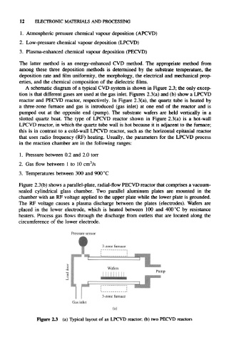
A schematic diagram of a typical CVD system is shown in Figure 2.3; the only excep-
tion is that different gases are used at the gas inlet. Figures 2.3(a) and (b) show a LPCVD
reactor and PECVD reactor, respectively. In Figure 2.3(a), the quartz tube is heated by
a three-zone furnace and gas is introduced (gas inlet) at one end of the reactor and is
pumped out at the opposite end (pump). The substrate wafers are held vertically in a
slotted quartz boat. The type of LPCVD reactor shown in Figure 2.3(a) is a hot-wall
LPCVD reactor, in which the quartz tube wall is hot because it is adjacent to the furnace;
this is in contrast to a cold-wall LPCVD reactor, such as the horizontal epitaxial reactor
that uses radio frequency (RF) heating. Usually, the parameters for the LPCVD process
in the reaction chamber are in the following ranges:
1. Pressure between 0.2 and 2.0 torr
3
2. Gas flow between 1 to 10 cm /s
3. Temperatures between 300 and 900 °C
Figure 2.3(b) shows a parallel-plate, radial-flow PECVD reactor that comprises a vacuum-
sealed cylindrical glass chamber. Two parallel aluminum plates are mounted in the
chamber with an RF voltage applied to the upper plate while the lower plate is grounded.
The RF voltage causes a plasma discharge between the plates (electrodes). Wafers are
placed in the lower electrode, which is heated between 100 and 400 °C by resistance
heaters. Process gas flows through the discharge from outlets that are located along the
circumference of the lower electrode.
Figure 23 (a) Typical layout of an LPCVD reactor; (b) two PECVD reactors